Finetech will showcase packaging equipment at Semicon
Finetech will present its FINEPLACER ® system solution at Semicon China 2010. This is a device developed for high-end micro-assembly / optoelectronic packaging / professional SMD rework.
The multi-function placement machine FINEPLACER ® pico ma is designed for prototyping or small batch production, R&D and university research institutes. It has a flip chip accuracy of better than 5μm and a modular design that supports almost all semiconductor chip packaging processes. Suitable for all process transfer from R&D to production, with powerful process observation and feedback capabilities, process development is very easy and results are reliable. FINEPLACER ® pico ma can process components from 0.125 x 0.125 mm2 to 100 x 90 mm2 in a working area of ​​up to 450 x 122 mm. It supports up to 8 wafer substrates.
The sub-micron micro-assembly platform FINEPLACER ® lambda is modular in design and offers outstanding flexibility for easy reconfiguration and use in different applications. With a manual platform or semi-automatic configuration, it is ideal for small batch production, prototyping, education and R&D that are critical to process flexibility.
FINEPLACER ® lambda is capable of handling components from 0.07 x 0.07 mm2 to 60 x 90 mm2 over a working area of ​​up to 300 x 73 mm. It supports up to 6 wafer substrates. This economical chip soldering unit can handle a variety of complex processes including indium soldering, eutectic soldering, thermal/ultrasonic soldering, gluing processes, and exceptionally sensitive materials such as GaAs or GaP.
At this exhibition, FINETECH will focus on how laser bars can achieve sub-micron assembly. The platform is capable of independently performing all of the laser bar assembly process steps - including pick and roll of laser bars, transfer of substrates or heat sinks, and placement and soldering with inert gas or formic acid vapor protection.
The FINEPLACER ® assembly platform covers not only the entire range of optoelectronic and microelectronic applications, such as the assembly and soldering of VCSELs/photodiodes/LED/MEMS and MOEMS or micro-optics, but also unmatched placement accuracy and huge applications. Flexibility for successful application in the most complex 3D, multi-chip and wafer level package (W2W, C2W) tasks.

YUANKAIDA Professional Custom OEM 3C Digital Peripheral Products, Circuit Board PCBA Design. Have A Professional Development And Design Team! According To Years Of Domestic And Foreign Related Product Design And Development Experience.
Product Concept, Combing, Evaluation, Market Research, Product Realization, Packaging. Having A Near-Perfect Solution That Helps You Quickly Seize The Market.
Custom 3C Digital Peripheral Products, OEM USB HUB , OEM Multi-Port USB Fast Charge, OEM USB HUB + Card Reader, OEM Usb Hub Sound Card, OEM Type-C HUB, OEM USB Card Reader, OEM USB Extension Cable, OEM Mobile Hard Disk Box And Other Circuit Board Design You Can Customize PCBA Of Different Sizes

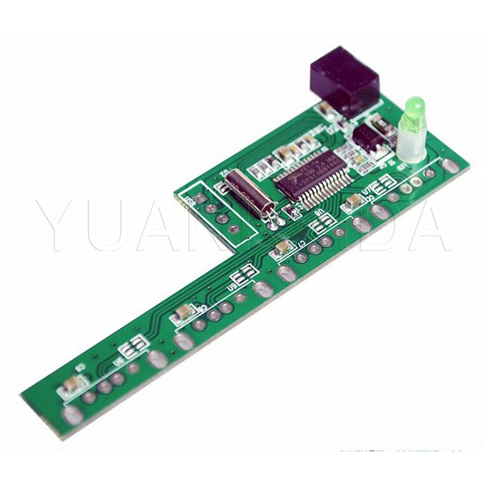
OEM USB HUB PCBA

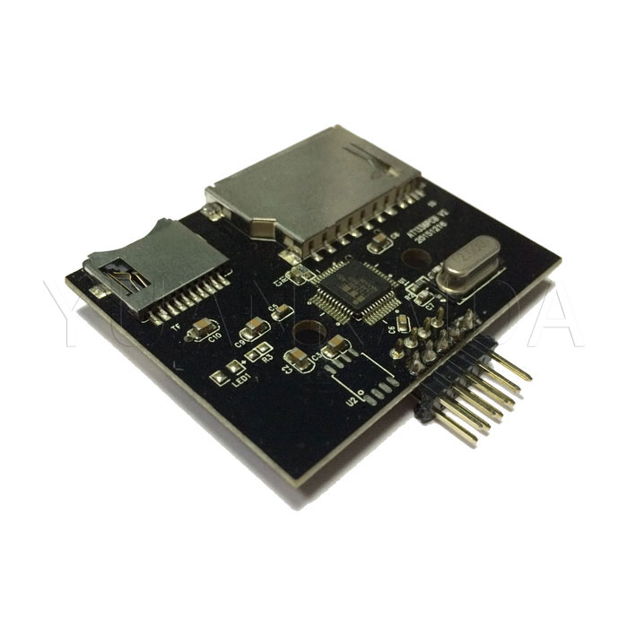
OEM Card Reader PCBA
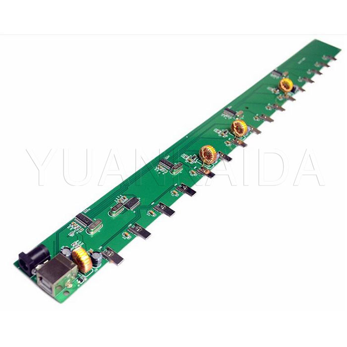
Customize USB Charging PCBA
OEM USB PCBA,OEM USB HUB,OEM Type-C HUB,OEM USB Card Reader,OEM USB Extension Cable
Shenzhen JunYuanJie Electronic Technology Co., Ltd. , http://www.usb3c.com
