How to debug digital hardware design?
Let's take a look at how to minimize any problems that can occur while advancing the design to a higher level, and how to get through the debugging phase quickly and smoothly.
I have to imagine how to test from the first day.
All engineers know that as the development process progresses, the cost of modifying the problem will increase accordingly. Once the design is finalized and put into production, the cost of modifying the pinout error is necessarily higher than the cost of the earlier design evaluation. In addition, there are also cost issues in testing and integration. The sooner you consider hardware, FPGA, system, etc. test problems and write test specifications, the easier it is for the engineering team to consider the necessary test points, connections, and functionality. The purpose of the test is to ensure that a safety system that meets the specific requirements of the user can be introduced. Therefore, we must ensure that the test reflects all requirements, while functional testing requires that process delivery be achieved and design requirements be tracked (ie, each test should meet its needs).
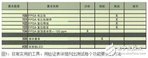
In addition, it is a good practice to edit the design verification model to detail the method of testing each functional requirement, such as a specific test, analysis or read method (provided that it is clear or tested earlier on another project). Related requirements). The documentation (Figure 1) may also cover which tests are required for design verification and which are used for production runs. Completing the above documentation early in the project phase ensures that the system design team and the test equipment design team get a clear, basic approach.
However, the design engineer must also ensure that the underlying hardware is correct before performing functional testing. They usually require hardware-level test specifications that include power, performance, and basic hardware verification, while hardware basic verification needs to be done before functional testing.
It is important to know which test equipment is needed and what kind of performance, such as the need to analyze the signal generator and logic analyzer to provide sufficient memory depth and operating frequency? In addition, you need to know if you need more specialized test equipment, such as arbitrary waveform generators, high stability frequency references, and so on.
What should be included in the design phase
In the hardware design process, perhaps several design features and functions should be included to make board testing more convenient. The relevant requirements may be simpler or deeper.
The simplest and most common test rule is to place test points on all voltage sources, which avoids the possibility of damage when interrogating solder joints. However, there is a better way to simplify the test by having the pad returning to ground (0V) close to the voltage test point. If a high value resistor is used to protect this test point, the current in the event of an unexpected short circuit in the test can be limited. We can also consider adding test pins to these pads to connect them to an automated test system that can then record results during production runs.
In addition, the ability to monitor the clock and reset the output is critical. Therefore, it is not a good idea to place test points on the reset line. In addition, you should ensure that the unused clock buffers are properly terminated and test points are added to facilitate interrogation of the clock. In addition, you can consider adding test ports to signal injection and extraction through signal generators, logic analyzers, or other test tools.
To help the prototyping meet power requirements, it is usually better to connect low-value resistors (10 milliohms, 100 milliohms, etc.) to the output of the voltage regulator, if possible, to accurately measure the current on the power rail.
A wide range of FPGA devices can also provide a way to monitor the temperature of the chip using a temperature diode. Need to find a way to provide a constant current to the diode. Measuring the chip temperature helps us ensure that the junction temperature does not exceed the rating.
Make sure that all components are properly seated to see if they meet the design requirements, especially if only one pull-up or pull-down resistor should be in place and the configuration mode is selected.
After checking the components on the printed circuit board, the next step is to power up the board for the first time. This is a very tense moment for any engineer. However, the test specifications developed during the design phase (test points, current sense resistors, etc.) will play a significant role in this. The first step is to ensure that the power output of the load point and other regulators does not short return. You may find low impedance on the power rail of the on-load device (with high current requirements), but the impedance should be greater than 1 ohm.
For the same type of design that the industry is the first to achieve (that is, the first time a new product is actually built), we should probably make more in-depth design decisions, such as separating the power supply from downstream electronics. In this way, we can ensure that the power supply and power-on sequence work properly, thus avoiding excessive stress or damage to downstream components. An example of a more detailed front-end design phase that helps test the test is to ensure that the JTAG port has more use than programming all FPGAs or processors in the system, such as by boundary scan testing. Initial hardware verification, etc. Boundary-scan testing is useful for reducing hardware design risk early in the testing phase, as well as optimizing the design to ensure maximum coverage of boundary-scan devices.
Diode TVS (Transient Voltage Suppressor), also known as Transient suppression diodes, is widely used a new type of high efficient circuit protection device, it has a fast response time (the nanosecond) and high surge absorbing ability.When it ends of stand moments of high energy shock, TVS can bring the two ends at high rate from high impedance to a low impedance between impedance values, to absorb a large current moment, put it at both ends of the voltage restraint on a predetermined value, thus protecting the back of the circuit components are not affected by the impact of the transient high pressure spikes.
Silicon TVS / TSS
Silicon TVS Transient Voltage Suppresso,Silicon TSS Transient Voltage Suppresso
YANGZHOU POSITIONING TECH CO., LTD. , https://www.yzpst.com