Detailed introduction of vertical structure LED chip
We know that LED chips have two basic structures, the lateral structure (Lateral) and the vertical structure (Vertical). The two electrodes of the lateral structure LED chip are on the same side of the LED chip, and the current flows laterally in unequal distances in the n- and p-type confinement layers. The two electrodes of the vertical structure LED chip are respectively on both sides of the LED epitaxial layer, and since the patterned electrode and the entire p-type confinement layer serve as the second electrode, the current flows almost entirely vertically through the LED epitaxial layer, and there is little lateral flow. The current can improve the current distribution of the planar structure, improve the luminous efficiency, and can also solve the problem of the P-pole shading and improve the luminous area of ​​the LED.
Let us first understand the manufacturing technology and basic methods of vertical structure LEDs:
There are three main methods for manufacturing vertical structure LED chip technology:
First, the use of silicon carbide substrate to grow GaN film, the advantage is that under the same operating current conditions, less light decay, long life, the disadvantage is that the silicon substrate will absorb light.
Second, the use of chip bonding and stripping technology. The advantage is that the light decay is small and the life is long. The disadvantage is that the LED surface needs to be processed to improve the luminous efficiency.
Third, the use of a heterogeneous substrate such as a silicon substrate to grow a gallium nitride LED epitaxial layer, the advantage is that the heat dissipation is good and easy to process.
There are two basic methods for fabricating vertical structure LED chips: stripping the growth substrate and not stripping the growth substrate. The vertical structure GaP-based LED chip grown on the gallium arsenide growth substrate has two structures:
The conductive gallium arsenide growth substrate is not stripped: a conductive DBR reflective layer is laminated on the conductive gallium arsenide growth substrate, and a GaP-based LED epitaxial layer is grown on the conductive DBR reflective layer.
Stripping a gallium arsenide growth substrate: a layered reflective layer on a GaP-based LED epitaxial layer, bonding a conductive support substrate, and stripping the gallium arsenide substrate. The conductive support substrate includes a gallium arsenide substrate, a gallium phosphide substrate, a silicon substrate, a metal and an alloy, and the like.
In addition, vertical GaN-based LEDs grown on silicon wafers also have two structures:
The silicon growth substrate is not stripped: a metal reflective layer or a conductive DBR reflective layer is laminated on the conductive silicon growth substrate, and the gallium nitride-based LED epitaxial layer is grown on the metal reflective layer or the conductive DBR reflective layer.
Stripping the silicon growth substrate: laminating the metal reflective layer on the gallium nitride-based LED epitaxial layer, bonding the conductive support substrate on the metal reflective layer, and stripping the silicon growth substrate.
The process of manufacturing a vertical gallium nitride-based LED is briefly described. The layered reflective layer is on the gallium nitride-based LED epitaxial layer, and the conductive support substrate is bonded on the reflective layer to peel off the sapphire growth substrate. The conductive support substrate includes a metal and alloy substrate, a silicon substrate, and the like.
Whether it is a GaP-based LED, a GaN-based LED, or a ZnO-based LED such as a through-hole vertical structure LED, it has a larger advantage than a conventional structure LED, and the specific performance is as follows:
1. At present, the existing vertical structure LEDs of all colors: red LED, green LED, blue LED and ultraviolet LED can be made into a through-hole vertical structure LED has a great application market.
2. All manufacturing processes are performed at the wafer level.
3. Since there is no need to connect the gold wire to the external power source, the thickness of the package of the LED chip with the vertical structure of the through hole is reduced. Therefore, it can be used to manufacture ultra-thin devices such as backlights and the like.
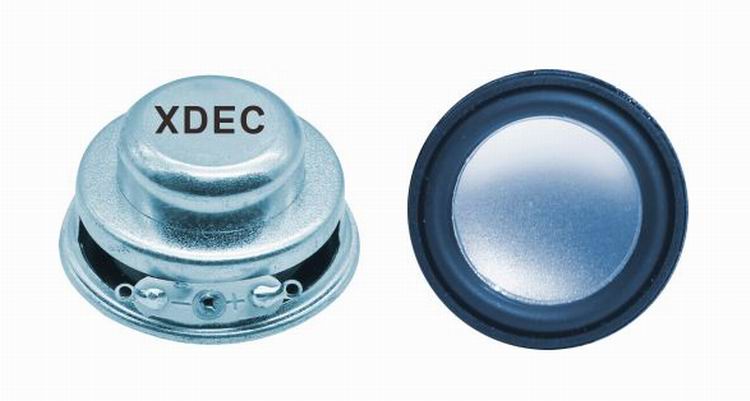
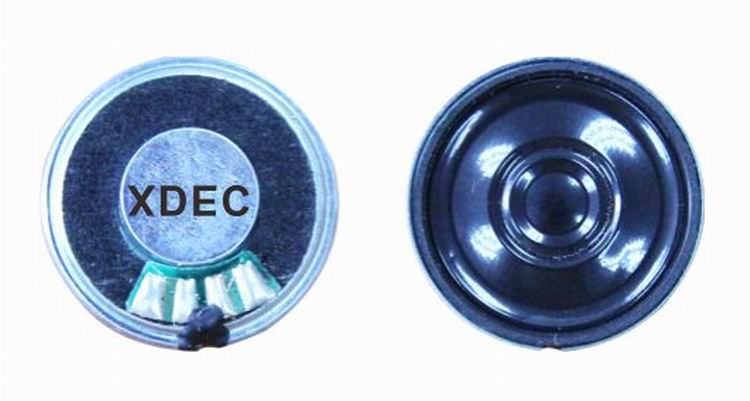
Waterproof speaker is a kind of speaker unit which is used for devices in waterproof demanded. They have loud sound, wide frequency response range and rich bass. We can customize waterproof speakers in IP65 and IP67.
Our main Multimedia Speakers are full ranges speakers units:
1) From the diameter: we have speakers in 1" ~ 3".
2) From the power output, we have speakers of 2W ~ 15W.


FAQ
Q1. What is the MOQ?
XDEC: 2000pcs for one model.
Q2. What is the delivery lead time?
XDEC: 20 days for normal orders, 15 days for urgent orders.
Q3. What are the payment methods?
XDEC: T/T, PayPal, Western Union, Money Gram.
Q4. Can you offer samples for testing?
XDEC: Yes, we offer free samples.
Q5. How soon can you send samples?
XDEC: We can send samples in 3-5 days.
Waterproof Speaker
Waterproof Speaker ,Mini Waterproof Speaker,Portable Waterproof Speaker,Bluetooth Waterproof Speaker
Shenzhen Xuanda Electronics Co., Ltd. , https://www.xdecspeaker.com