Three solutions for high-side current sensing with wide dynamic range (1)
In many applications such as motor control, solenoid control, communication infrastructure, and power management, current sensing is a critical feature required for precision closed-loop control. How to design a wide dynamic range of high-side current-sense circuits is challenging for most engineers. Here are a few recommended circuits from ADI technologists Neil Zhao, Wenshuai Liao, and Henri Sino for your reference.
Three alternative solutions are presented in order of design complexity from high to low, which provide viable high-accuracy, high-resolution current sensing for a wide range of applications.
1. Construct a current sensor using discrete devices such as op amps, resistors, and Zener diodes. This solution is based on the AD8628 zero-drift amplifier.
2. Use high-voltage bidirectional shunt monitors such as the AD8210 to increase integration and use other external components to extend dynamic range and accuracy.
3. Use device-optimized devices such as the newly introduced AD8217. The AD8217 is an easy-to-use, highly integrated zero-drift current sensor with an input common-mode voltage range of 4.5 V to 80 V.
Solution 1: Configure a standard op amp for high-side current sensing
Figure 1 shows an op amp-based discrete solution using the AD8628. The same settings are valid with other op amps, but must have the following characteristics: low input offset voltage, low offset voltage drift, low input bias current, and rail-to-rail input-output swing capability. Other recommended amplifiers include the AD8538, AD8571, and AD8551.
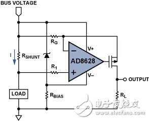
This circuit monitors the high side current I. The amplifier is biased open by a Zener diode, which is rated at 5.1 V in this example. The use of a diode ensures that the amplifier can operate safely at high common-mode levels, and its supply voltage is stable within acceptable power limits, while the MOSFET converts its output into a current that is converted from a RL to a ground-referenced Voltage. In this way, the output voltage can be fed to converters, analog processors, and other ground-referenced devices such as operational amplifiers or comparators for further signal conditioning.
In this configuration, the voltage on RG is equal to the voltage on RSHUNT because the feedback from the MOSFET keeps the two high-impedance inputs of the op amp at the same voltage. Current through RG flows through the FET and RL, producing VOUTPUT. The relationship between the current I flowing through the shunt resistor and VOUTPUT can be expressed by Equation 1:
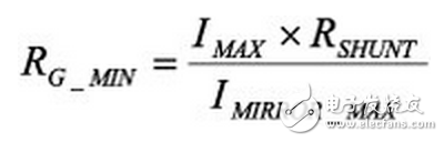
RSHUNT Selection: The maximum value of RSHUNT is determined by the allowable power dissipation at maximum current, while the minimum value is determined by the op amp's input range and error budget. In general, to monitor currents above 10 A, the value of RSHUNT is between 1 mΩ and 10 mΩ. If a single resistor does not meet the power requirements or is too large for the PCB, RSHUNT may have to consist of multiple resistors in parallel.
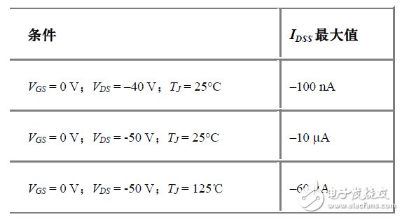
RG Selection: RG is used to convert the current proportional to the high side current to the low side. The maximum value of RG is determined by the drain-source leakage current of the P-channel MOSFET. Assuming the common P-channel enhancement type vertical DMOS transistor BSS84 is used, the maximum IDSS under various conditions is shown in Table 1.
Table 1. Drain-Source Leakage Current
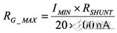
The minimum value of RG is determined by the allowable mirror current power dissipation at maximum load current:
RBIAS selection: The current through the RBIAS is shunted to produce the quiescent current of the op amp and a substantially constant Zener diode voltage VZ (which determines the op amp's supply voltage). When the amplifier current ISUPPLY is actually 0 and VIN is at its maximum, ensure that the current flowing through the Zener diode does not exceed its maximum regulation current, IZ_MAX:
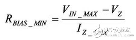
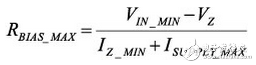
When ISUPPLY is at its maximum and VIN is at its minimum, to ensure that the diode voltage is stable, the current flowing through it should be greater than its maximum operating current IZ_MIN:
Zener diodes and RBIAS are key components of this solution because they eliminate the high common-mode voltage of subsequent circuits and support the use of low-voltage precision op amps. In order to maintain the highest voltage stability, Zener diodes should have low dynamic resistance and low temperature drift characteristics.
R1 Selection: R1 is used to limit the amplifier input current when the input transient exceeds the op amp's supply voltage. A 10 kΩ resistor is recommended.
The offset voltage VOS and offset current IOS of the selected op amp are very important indicators, especially if the shunt resistor value and load current are low. VOS + IOS & TImes; R1 must be less than IMIN &TImes; RSHUNT, otherwise the amplifier may be saturated. Therefore, for best performance, it is best to use a rail-to-rail input amplifier with zero crossover distortion.
Another issue to consider for this discrete solution is temperature drift. Even with zero-drift amplifiers, it is very difficult to optimize, or it can be costly to optimize the drift caused by the following discrete devices: Zener diodes, MOSFETs, and resistors. As can be seen from Table 1, when VGS = 0 V and VDS = –50 V, the IDSS maximum value of the MOSFET changes from –10μA to –60 μA as the operating temperature changes from 25°C to 125°C. This drift reduces the accuracy of the system over the entire temperature range, especially when the monitored current is low. The drift characteristics of the Zener diode affect the stability of the amplifier supply, so the amplifier used should have high power supply rejection (PSR) performance.
In addition, designers must be aware that this solution is inefficient because RBIAS consumes a lot of power. For example, if the bus common-mode voltage is 28 V, the Zener diode output voltage is 5.1 V, and the RBIAS is a 1000 Ω resistor, the circuit's useless power consumption will exceed 0.52 W. This will increase the power budget and must be considered when designing.
yucheng county huibang electric technology ltd , https://www.hbspeaker.com