High-power LED packaging technology detailed (Figure)
The power driven by the LED package is limited by the thermal resistance of the package and the associated thermal module (Rca), which determine the maximum power value that the LED 's system thermal resistance and steady state can tolerate. In order to reduce the thermal resistance of the package, the operator tries to increase the distribution distance of the LED crystal in the package. However, the LED die area is not too large. The excessive light-emitting area makes the subsequent optics difficult to handle and limits the application of the product. It is not necessary to package more LED chips in a single body in order to achieve high power packaging, because there are still many factors to be considered, especially for the application surface.
Multi-die package materials continue to evolve
As the LED package power increases, the multi-chip package becomes a trend. The traditional high-power LED package adopts the plastic pre-mold lead frame (Fig. 1a), and the package carrier ( Carrier), also known as Die Pad, is a continuous metal block that cannot meet the electrical requirements of multi-die serial connection. The electrical series-parallel method directly affects the LED die electrical measurement bin (Bin). Precision, reliability life, and drive circuit design required for the package to be applied. Therefore, many LED package types have been proposed one after another. Figure 2 shows typical examples of several representative high-power LED packages.
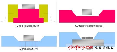
Figure 1 shows the structure of common high-power LED package

Figure 2 Typical representative high power LED package
Aluminum Die Casting,Aluminum Die Casting Parts,Aluminium Die Casting Process,Aluminium Die Casting
Dongguan Formal Precision Metal Parts Co,. Ltd , https://www.formalmetal.com