With the advancement of 4G/5G mobile communication technology, the demand for antenna-compatible multi-band systems has significantly increased. In the design process, it is crucial to test the standing wave ratio (SWR) and insertion loss of the antenna. However, using a network analyzer for manual plugging and unplugging is not only time-consuming but also prone to errors due to repeated connections, which can lead to poor contact performance and make it difficult to verify the accuracy of the design. Therefore, an automated testing method is necessary to replace manual wiring tests. This approach allows for expanding the network test ports and docking them with the antenna test ports. However, during the design process, various challenges may arise, and the following step-by-step analysis will help address these issues.
**Problem Phenomenon**
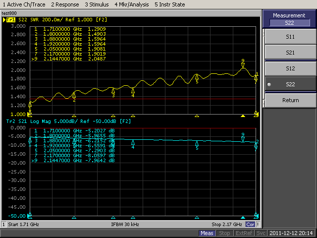
During the antenna testing phase, it was observed that one of the channels exhibited abnormally high SWR and insertion loss. The maximum SWR reached 3.1, and the differential loss was as high as 20 dB. Upon investigation, it was determined that the issue stemmed from excessive SWR and insertion loss at one of the PCB ports.
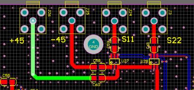
By comparing the results, it was found that when the -45° port was used as the input and the S11 port as the output, both SWR and insertion loss were within normal limits, with a maximum SWR of 1.53 and an insertion loss of -7 dB. However, when the +45° port was the input and the S22 port was the output (as shown in Figure 1), the maximum SWR increased to 3.2, and the insertion loss reached 20 dB. Despite having the same circuit structure, the difference lay in the length of the transmission line. After analysis, it was concluded that the high SWR and insertion loss were caused by impedance mismatch in the circuit. The next step was to resolve this issue.
**Single Port Solution**
1. Option 2: Replace the antenna switching IC. Based on current performance, only the HMC595E meets the requirements (though it could also be replaced with a PIN diode).
2. Option 3: Modify the circuit design to match the transmission line. This option is feasible.
**Multiport Testing**
The goal of this test was to identify and solve the issue where ICs interacted with each other, causing deterioration in SWR and insertion loss.
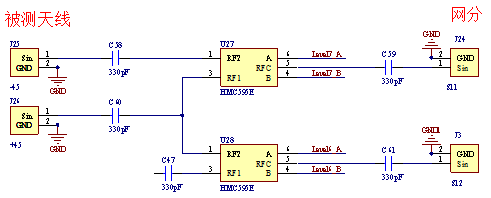
- **Test 1:** +45° IN, S22 OUT; other ports left floating. Levels: U27_A low, U27_B high, U28_A high, U28_B low.
- **Test 2:** +45° IN, S22 OUT; other ports left floating. Levels: U27_A high, U27_B low, U28_A high, U28_B low.
- **Test 3:** -45° IN, S11 OUT; other ports left floating. Levels: U27_A high, U27_B low, U28_A low, U28_B high.
- **Test 4:** +45° IN, S11 OUT; other ports left floating. Levels: U27_A low, U27_B high, U28_A high, U28_B low.
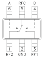
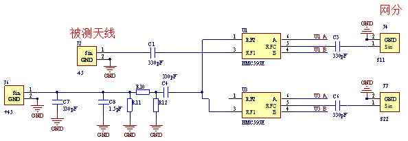
In Test 2, we aimed to evaluate the impact of U27 on the SWR and insertion loss of the U28 path. According to theoretical analysis, when U27_A is high and U27_B is low, the U27_RF1 pin is disconnected, while U27_RF2 is connected. Similarly, when U28_A is high and U28_B is low, the U28_RF1 pin is disconnected, and U28_RF2 is connected (see Figure 4 for pin diagram and truth table).
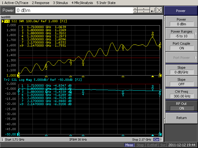
After soldering U27, the SWR of the S22 port increased slightly, reaching a maximum of 2.1, compared to 1.7 before welding. This indicated that the presence of U27 had a minor impact on the signal path.
To address the impedance mismatch, the circuit was modified to ensure proper matching during signal transmission. After debugging, the final circuit configuration was as follows:
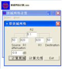
In Figure 7, R10 = 5.1 Ω, R11 = R12 = 810 Ω, achieving a 50 Ω impedance match. The specific calculations can be done using network attenuation calculation software, as shown below.
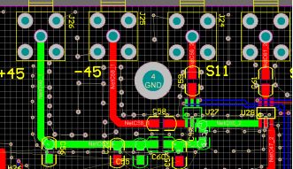
The modified PCB layout is illustrated below:
**Partial Standing Wave Test Data**
| Channel | Board Port | Antenna | System |
|--------|------------|---------|--------|
| S22 | 1.54 | 1.51 | 1.78 |
| S11 | 1.55 | 1.44 | 1.58 |
**Summary**
This method temporarily resolves the SWR and insertion loss issues, but it does not provide precise values for the circuit parameters or PCB layout, which limits efficiency. In the next article, we will explore the root causes of the problem in greater detail.
ELF WORD
Original Elfworld Disposable supplier from china,Elfworld series contain :Elfworld DC5000 ,Elfworld DE6000,Elfworld CAKY 7000,Elfworld TRANS 7500 and so on.Elfworld DC5000 Disposable Device Pen similar Elf Bar ultra 5000.Elfworld DE6000 Modern E-cigarette very fashion style design.Elfworld CAKY 7000 Disposable Vape Pen Stick get good price and beautiful version.Elfworld TRANS 7500 Vape Pen Disposable E Cigarette is the new style now.welcoem contact with us ,get good price and best service .
Elfworld DC5000 Ultra ,Elfworld Caky7000 Disposable Vape,Elfworld Disposable Vape,Elfworld DE6000,Elfworld Trans 7500
Shenzhen Ousida Technology Co., Ltd , https://en.osdvape.com