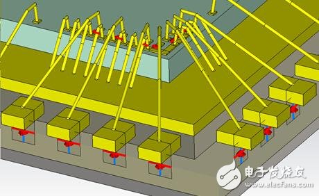
How do high-performance analog-to-digital converters have many power connections with only a small amount of grounding?
How do high-performance analog-to-digital converters manage to have numerous power connections while using only a limited number of ground connections? The answer lies in the design of the package and how it handles both thermal and electrical requirements. One effective solution is the lead frame chip scale package (LFCSP) with an exposed die pad, or the quad flat package (QFP). These packages provide a direct thermal path from the component to the PCB, significantly reducing thermal resistance. The exposed die pad is not encapsulated and must be soldered directly to the PCB, acting as an integrated heat sink.
A well-designed PCB should include a dedicated pad for the exposed die pad. This pad should be connected via an array of vias to multiple ground planes on the board, creating a low-thermal-resistance path for heat dissipation. This design not only improves thermal performance but also enhances electrical grounding by allowing the die pad to serve as a ground connection within the package itself.
By using the exposed pad for grounding, the package gains more flexibility and efficiency. Instead of routing ground signals through traditional package pins, these signals are directly connected from the chip’s ground pad to the die pad. This configuration reduces the overall inductance and provides a low-impedance path for current flow. Experienced engineers understand that high-performance ICs often place power and ground pins next to each other to form a tightly coupled loop, minimizing inductance and improving signal integrity.
In mixed-signal systems, transient currents from digital switching, I/O activity, and analog signal variations can cause noise on power lines or interfere with sensitive analog components. Proper grounding helps control these effects by forming low-inductance loops without requiring extra package leads. This frees up other pins for additional functions, such as power supply, signal routing, or auxiliary connections.
However, many users are confused about how ADCs and DACs achieve high performance with minimal ground pins. Some devices even lack dedicated ground pins, relying entirely on the exposed pad for all ground connections. This makes proper PCB layout and thermal management essential for optimal performance.
LLP package with ground wire
High Voltage Capacitor Charging Power Supplies
High Voltage Capacitor Charging is a mainstream application of high-current high-voltage power supplies. The High-voltage Capacitor Charging power supplies are a kind of high-voltage DC Power Supplies specially designed to meet the requirements of capacitor charging or capacitor conditioning.
At present, iDealTek-Electronics' high-voltage capacitor charging power supplies are IGBT-based switching mode High Voltage Power Supplies. Compared with the traditional linear high-voltage power supplies, the switched-type capacitor charging high-voltage power supplies are featured for higher power density, higher efficiency, higher output response speed and faster protection start and self-recovery speed.
iDealTek-Electronics originally produced linear capacitor charging high-voltage power supplies. Based on years of experience in the capacitor industry, our current capacitor charging high voltage power supplies use 19-inch standard racks, 4U and 6U chassis, which facilitate the installation of integrated capacitor charging systems. The output power ranges from 2KW to 10KW with output voltage levels at 5KV / 10KV / 20KV / 30KV / 35KV / 40KV / 50KV / 60KV / 100KV with a complete protection function, which can deal with overvoltage, overcurrent, load discharge and other situations.
The output voltage and current of the power supply can be controlled and read through the front operation panel of the power supply. And, this series of high voltage capacitor charging power supplies are also equipped with RS485 / DB15 / DB50 interfaces as standard. Customers can edit the control software according to our communication protocol or apply 0-10V signals and dry contact signals on the interface according to the definition of the analog interface to achieve full control and monitoring of the power supply, such as high voltage start/stop, output settings and readings.
HV Capacitor Charging Power Supplies, High-voltage Capacitor Charging Power Supplies, Capacitor Charging High Voltage Power Supplies, Capacitor Charging HVPS, HV Capacitor Charger
Yangzhou IdealTek Electronics Co., Ltd. , https://www.idealtekpower.com