VDD and VSS clamp diodes in series and series resistors for protection
In this article, we do not deal with EMC's design recommendations. However, at the component level, the "latch" phenomenon inherent in the technology used is the only factor considered.
The CMOS structure package consists of a PNPN thyristor type cell that is generated by parasitic transistors between VDD and VSS. When the parasitic thyristor is disturbed and activated, causing a short circuit to the μC's power supply, and causing damage to the internal structure, a delay occurs. The following conditions may cause "latch":
ü The voltage of the input/output voltage is higher than VDD or lower than VSS.
ü Power supply voltage VDD is higher than VDDMax
ü Power supply VDD changes dramatically.
The μC is protected against static electricity. The input is internally configured to protect the network, protected by VDD and VSS clamp diodes and series resistors in parallel.

However, this internal protection circuit must be completed at the design level. Suggest:
ü Maintain the supply voltage of μC within its rated range.
ü Use low-pass filter to connect input signal with high frequency signal
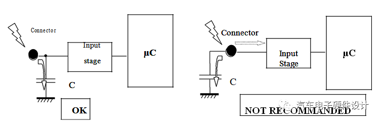
ü Place an electrostatic capacitor directly on the connector pins for protection.
Uv Curving Glass,Tempered Glass Screen Protector,Film Cutting Machine,Uv Curing Protector Screen
Shenzhen TUOLI Electronic Technology Co., Ltd. , https://www.hydrogelprotector.com