The basis of the analog circuit
So how can Analog go to Digital?
First, several steps of the ADC
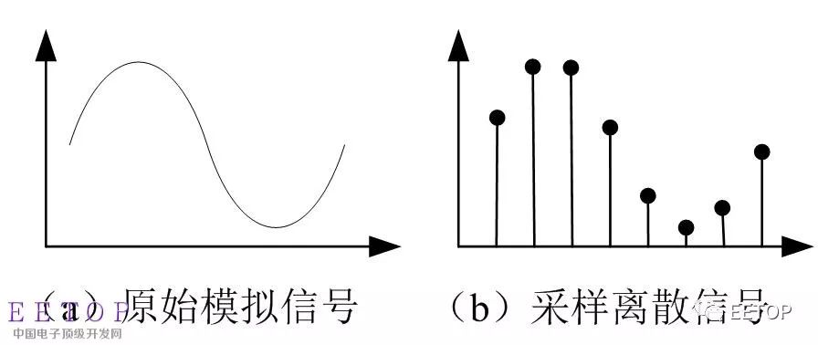
1, sampling and maintenance
If we compare analog signals to digital signals with infinite sampling points, then we need to take some of these finite points for true digital transmission. How many points do you take? How to pick?
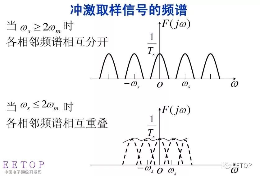
Nyquist sampling theorem:
Simply put, the sampling frequency must be greater than twice the signal frequency, fs ≥ 2fn. This will restore the signal. If not, it will not be able to recover due to spectrum aliasing. The specific reason is to find the formula to derive and analyze. Spectrum as shown below
The simple meaning of keeping is to save the sampled values ​​to the next step.
2. Quantization and coding
The so-called quantification is to convert the sampled N-point values ​​into digital 0 and 1 according to certain standards and steps. This process can be divided into many ADC types according to different modes, so it has different performance characteristics, see below. .
Second, several architectures of ADC
1, integral ADC
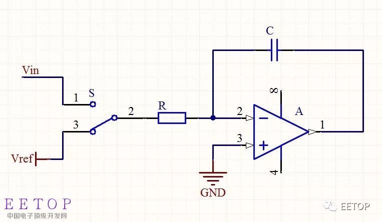
As the name implies, the basic principle of the integral ADC is to use the op amp to integrate the input signal and the reference signal. Here, the reference signal is generally opposite in polarity to the input signal, so that the output voltage has rise time and fall time, and the time is counted according to the counter. Finally, the value of the sampled signal is obtained according to the function relationship.
Feature introduction:
A: The integration time determines the conversion accuracy, so sacrificing the conversion speed can improve the accuracy. It is applied in some occasions where the accuracy of some instrument conversion is not high. Later ADCs rarely use this architecture.
B: Strong anti-noise ability. For white noise with positive and negative zero points, the integration can be eliminated.
2, successive comparison SAR
As the name implies, the output digital quantity is converted by comparison. The value used for comparison is generated by the DAC. As shown in the figure below, the output of the initialization DAC is set to 1/2Vref by the register, and then the size of the comparator determines the output to determine the output 1 or 0. Then proceed to the next step to set the register output DAC again, thus looping to the last LSB. The 0 and 1 output in sequence are the converted digital quantities. The core of the algorithm is the binary search, similar to the game of guessing numerical values.
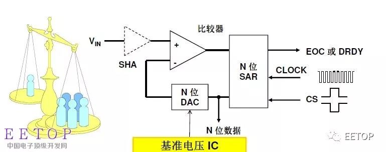
Feature introduction:
A: Medium speed of 100K to 1M, medium precision of 12 to 16 bits, and good overall performance, so it is one of the most widely used ADC architectures.
B: Accuracy is mainly determined by the conversion accuracy of the DAC, so the DAC needs to be calibrated, and the comparator also needs to meet the high speed and high accuracy of the matching system.
C: Power consumption is adjustable, which is determined by the conversion speed, thus limiting high speed applications.
D: In summary, the internal components of the SAR ADC require optimal combination performance matching.
3, Pipeline pipeline ADC
The basic principle is shown in the figure, using multiple comparators for parallel processing, obviously, high speed!
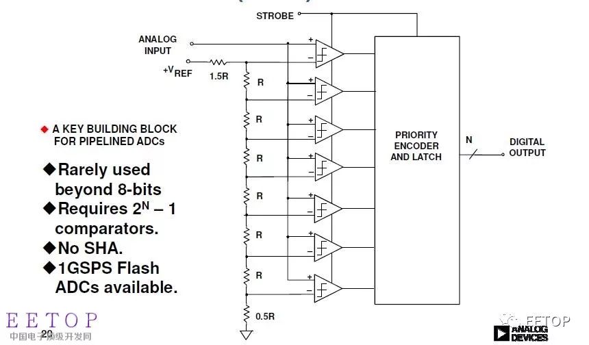
Feature introduction:
A: It is obviously fast enough, and the comparators are processed in parallel.
B: The power consumption is large and the area is large, naturally because there are many comparators.
C: The resolution is not enough, because the power consumption is large, and most of them are less than 16 bits.
D: The conversion cycle needs to be calibrated continuously to ensure a certain accuracy.
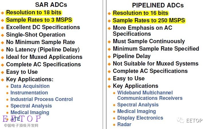
Comparison of two ADC architectures:
4, Σ-Δ ADC
The Sigma-Delta ADC is also a widely used ADC architecture, especially in high-resolution ADC designs. This modulation ADC conversion design uses digital circuitry to process and combine algorithms to achieve better results. performance. Core technology points: oversampling and noise shaping.
Sigma-Delta modulation oversampling:
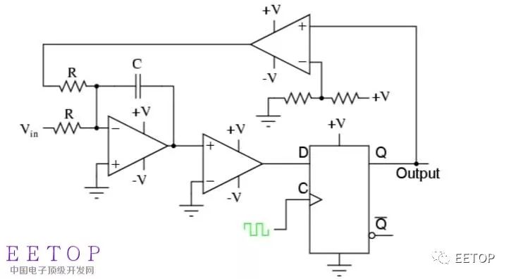
As shown in the figure, sigma-delta means differential summation. Let's take a look at this process as its name suggests:
Assuming the first integral op amp output is 1, the Q output is also 1 after the second, and the second op amp output is +V.
+V feedback to the first op amp input, driving the integrator to output in the opposite direction, and the signal Vi to be driven will also drive the integrator output. In general, if the integrator output is 0, the second comparator returns it - V, to drive the integrator to the output. The final purpose of this loop is to achieve the basic characteristics of the op amp: the inverting end should be 0!
Thus, the voltage value corresponding to the ratio of the number of 1 of the entire output is actually the voltage value of the signal to be tested! Can you understand? It is through the continuous accumulation of the error to get the corresponding value! Q will output a string of 01 values ​​to complete.
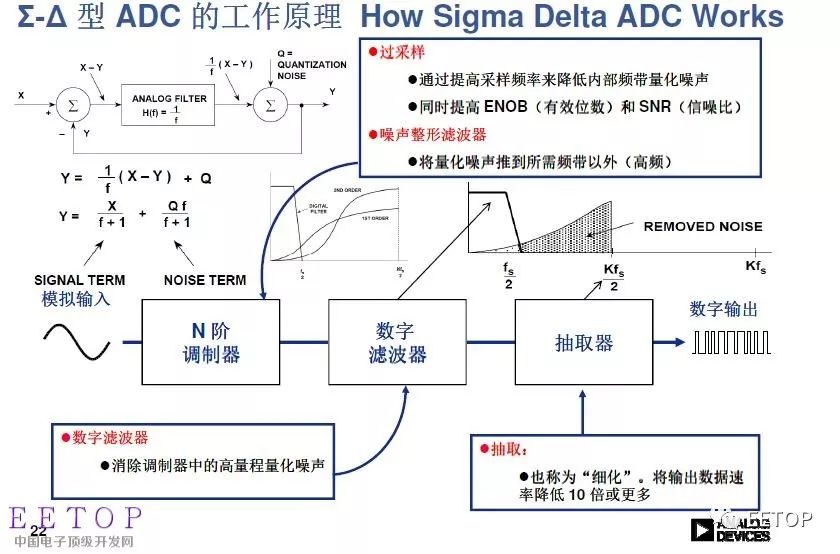
Oversampling:
The trigger clock in the above process is very fast, much larger than the Nyquist sampling requirement, so that the quantization noise can be pushed to a higher frequency band. Quantization noise: The error in the smallest unit of digital quantization is called quantization noise, which is the error value between 1LSB and 2LSB.
Noise shaping:
The high-speed 01 digital stream obtained in the previous step can be processed digitally to obtain the final output. Because it is operated in the process of over-sampling in terms of speed and accuracy, high speed but high noise, the noise is eliminated by the digital filter and the decimation circuit in the noise shaping process, and the final signal output rate is reduced to achieve high-precision data. Conversion result!
As summarized in the following figure:

A simple comparison of several ADC architectures:

Third, the parameters of the ADC
1, resolution
It is the minimum resolvable analog voltage value, such as a 12-bit ADC, Vref is 3.3V minimum resolution: Vref/2 is 12th power = 0.8mv.
2, conversion speed
That is, the digital quantity converted per second, such as 100kSPS, is also often expressed as the conversion time of each digital quantity such as 15us
3, the output interface
Serial or parallel interface
4. Operating voltage, reference voltage (internal or external reference), package.
, 5, DNL differential nonlinear error

6. INL integral nonlinearity error
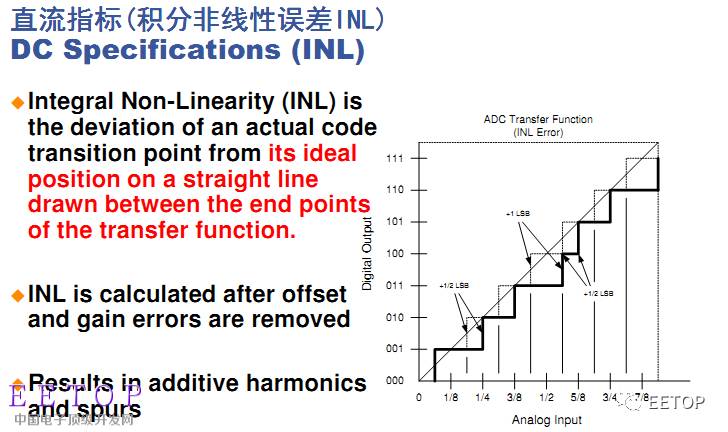
These two errors have some randomness, so the ADC will have a bit error.
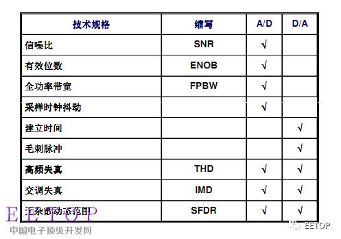
7, several important communication parameters
Fourth, the application of ADC
I originally wanted to use my very shallow experience to briefly talk about the main points of ADC application design, but I still can't write it. Maybe you don't like engineers to tell others about the situation, but after work, I find it more and more. You can't explain one item. All points of the application design, different characteristics and combinations of different applications are also very different in different operating environments. Your best way is to master a certain foundation and then fully think and verify.
As far as the ADC is concerned, the design naturally starts from the selection, what kind of signal to be tested, what kind of rate requirements, accuracy requirements, etc., which can be selected according to the previous knowledge. This process avoids blind design and wastes performance and cost. The accuracy of the ADC is naturally relative to the reference voltage, then the reference voltage should be stable, the power supply should be stable, the crystal oscillator as the clock should be stable, the PCB design should be handled well, the high-speed signal should be matched well, and the interference should be isolated. There are N multi-configuration options on the software to be appropriate, etc., the knowledge is shallow, can not be a little glimpse.
V. Summary
ADC is one of the most important links in the signal processing process. It is a bridge between analog and digital. The current signal processing is moving toward higher detection accuracy and faster conversion rate. It is applied in audio and video interfaces and weak signal detection. In-depth, and the localization of such chips is still far behind, but the future is expected. For the application in hardware development, knowing it and knowing why it has a better level of grasping the application, in time, perhaps in the end, it can reach the sword in the hands of martial arts, without a sword in the heart, The realm of the blade.

| About Enameled Copper Wire |
Henan HuaYang Copper Group Co.,Ltd specialized in producing enameled copper wire for 25 years ,Products including PEW enameled copper wire, EIW Enameled Copper Wire, EI/AIW enameled copper wire, EIW/A Enameled Copper Wire,and Enameled and glass-fiber copper wire.
According to the characteristics of motor, transformer, automotive electrical and high-speed winding machine, we have advantages in resilience, breakdown voltages and have imported machine to protect the quality of Enameled copper wire.
After 25 years of efforts, we have good reputation from foreign and domestic.

Product Feature.
Enameled
Copper Wire
Conductor
Copper
Dimension
Diameter(mm):
0.15 ~ 3.0
Thermal
Class(℃)
130(Class
B); 155(Class F); 180(Class H); 200(Class C); 220(Class C+);
Standard
IEC;
Packing
PT4
– PT200 or ply-wood spool
Application
Transformer;
motor; generator; modern instrument; welding machine and so on
About
Factory.
For quality of Enameled Copper Wire, we have imported machine and R&D. we checked every spools of products after finishing the products.


'Quality and efficiency' is our principle.
Enameled Copper Wire,Enameled Magnetic Copper Wire,Rewding Enameled Copper Wire,Winding Enameled Copper Wire
HENAN HUAYANG ELECTRICAL TECHNOLOGY GROUP CO.,LTD , https://www.huaonwire.com