Temperature measurement and data acquisition system MAX1358-Measuring T
IntroductionThe MAX1358 data acquisition system can measure temperature using an internal or external transistor PN junction. Figure 1 shows the internal temperature circuit and the external circuit. A constant current is supplied by the current source to produce a voltage (VBE) across the transistor. The current source can be programmed to produce up to four currents. For each current the voltage drop across the transistor is measured using the integrated ADC. The ADC has inputs for TEMP +, TEMP-, AIN1, AIN2, and AGND. These measured values ​​are used in an equation to determine the junction temperature.
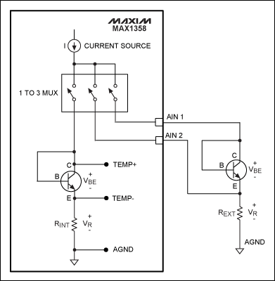
Figure 1. MAX1358 internal / external temperature measurement circuit.
Internal Four-Current MethodThe internal four-current method requires eight measurements to be used in the temperature-measurement equation. Equation 1 below is used for four-current measurement.
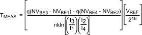
Equation 1. Four-current temperature measurement equation.
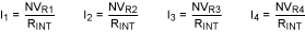
Substituting for I1, I2, I3, and I4 in the denominator:
Where:
TMEAS = temperature in Kelvin
q = electron charge = 1.60219 × 10⁻¹⁹ coulombs
NVBE1 = ADC reading with I1 as current source
NVBE2 = ADC reading with I2 as current source
NVBE3 = ADC reading with I3 as current source
NVBE4 = ADC reading with I4 as current source
VREF = ADC reference voltage = 1.251V (typ)
n = diode ideality = 1.000 (typ)
k = Boltzmann's constant = 1.3807 × 10⁻²³ Joules / Kelvin
I1 = Current source low setting (4µA)
I2 = Current source high setting (60µA)
I3 = Current source high setting (64µA)
I4 = Current source high setting (120µA)
NVR1 = ADC reading with I1 as current source
NVR2 = ADC reading with I2 as current source
NVR3 = ADC reading with I3 as current source
NVR4 = ADC reading with I4 as current source
216 = Number of ADC steps for MAX1358 16-bit ADC
To convert the measured temperature in Kelvin to degrees Celsius, the following formula is used:
° C = K-273.15
Procedure Using the Internal TransistorThe procedure for measuring the voltages across the internal transistor and internal resistor applies a current from the current source, and measures the resulting VBE and VR.
Step 1. Enable the Reference and ADCEnable the internal 1.251V reference and the reference buffer with a gain of 1.0 by setting REFV [1: 0] bits to 0x01 in the REF_SDC register.
Enable the ADC by setting the ADCE bit in the ADC register. The internal reference and ADC are enabled. Note: The ADC is set with the default parameters of unipolar, normal polarity, single conversion, internal reference, unity gain, 10 samples per second , and normal conversion.
Step 2. Calibrate the ADCSet the ADC conversion mode to Self Offset and Gain Calibration by setting the Mode [2: 0] bits to 0x07 in the ADC register. Start an ADC conversion by setting the STRT bit in the ADC register. The ADC is now calibrated. The Mode [2: 0] bits in the ADC register are automatically cleared. This returns the ADC to normal operation.
Step 3. Set the Current Source for the Internal Temperature SensorSet the current source for the internal temperature sensor by setting the IMUX [1: 0] bits to 0x01 in the TEMP_CTRL register.
Step 4. Set the Current Source for I1 (4µA) Set the current source for I1 by setting the IVAL [1: 0] bits to 0x00 in the TEMP_CTRL register.
Step 5. Set the ADC Input for TEMP + to TEMP-Set the ADC positive input multiplexer for TEMP + by setting MUXP [3: 0] to 0x07 in the MUX register. Set the ADC negative multiplexer for TEMP- by setting MUXN [3: 0 ] to 0x00 in the MUX register.
Step 6. Measure VBE1 Using the ADCThe VBE1 voltage is measured from the TEMP + to the TEMP- inputs to the ADC. The ADC is already configured and only needs to convert to get the resulting VBE1 voltage. To start the ADC conversion, set the STRT bit in the ADC register. The ADC will do a conversion and the result will be in the DATA register. Read the DATA register value and save as a 16-bit integer named VBE1 for later calculation.
Step 7. Set the ADC Input for VR1 Set the ADC positive input multiplexer for AGND by setting MUXP [3: 0] to 0x09 in the MUX register. Set the ADC negative multiplexer for TEMP- by setting MUXN [3: 0] to 0x00 in the MUX register (same as step 5). To measure the TEMP- input relative to AGND, the polarity flipper bit is used. Set the POL bit in the ADC register. The ADC is now setup with TEMP- as its positive input and AGND as its negative input.
Step 8. Measure VR1 Using the ADCTo start the ADC conversion, set the STRT bit in the ADC register. The ADC will do a conversion and the result will be in the DATA register. Read the DATA register value and save as a 16-bit integer named VR1 for later calculation.
Step 9. Set the Current Source for I2 (60µA) Set the current source for I2 by setting the IVAL [1: 0] bits to 0x01 in the TEMP_CTRL register.
Step 10. Set the ADC Input for TEMP + to TEMP-Set the polarity flipper back to normal by clearing the POL bit in the ADC register. Set the ADC positive input multiplexer for TEMP + by setting MUXP [3: 0] to 0x07 in the MUX register. Set the ADC negative multiplexer for TEMP- by setting MUXN [3: 0] to 0x00 in the MUX register.
Step 11. Measure VBE2 Using the ADCThe VBE2 voltage is measured from the TEMP + to the TEMP- inputs to the ADC. The ADC is already configured and only needs to convert to get the resulting VBE2 voltage. To start the ADC conversion, set the STRT bit in the ADC register. The ADC will do a conversion and the result will be in the DATA register. Read the DATA register value and save as a 16-bit integer named VBE2 for later calculation.
Step 12. Set the ADC Input for VR2Set the ADC positive input multiplexer for AGND by setting MUXP [3: 0] to 0x09 in the MUX register. Set the ADC negative multiplexer for TEMP- by setting MUXN [3: 0] to 0x00 in the MUX register (same as step 5). To measure the TEMP- input relative to AGND, the polarity flipper bit is used. Set the POL bit in the ADC register. The ADC is now setup with TEMP- as its positive input and AGND as its negative input.
Step 13. Measure VR2 Using the ADCTo start the ADC conversion, set the STRT bit in the ADC register. The ADC will do a conversion and the result will be in the DATA register. Read the DATA register value and save as a 16-bit integer named VR2 for later calculation.
Step 14. Set the Current Source for I3 (64µA) Set the current Source for I3 by setting the IVAL [1: 0] bits to 0x10 in the TEMP_CTRL register.
Step 15. Set the ADC Input for TEMP + to TEMP-Set the polarity flipper back to normal by clearing the POL bit in the ADC register. Set the ADC positive input multiplexer for TEMP + by setting MUXP [3: 0] to 0x07 in the MUX register. Set the ADC negative multiplexer for TEMP- by setting MUXN [3: 0] to 0x00 in the MUX register.
Step 16. Measure VBE3 Using the ADCThe VBE3 voltage is measured from the TEMP + to the TEMP- inputs to the ADC. The ADC is already configured and only needs to convert to get the resulting VBE3 voltage. To start the ADC conversion, set the STRT bit in the ADC register. The ADC will do a conversion and the result will be in the DATA register. Read the DATA register value and save as a 16-bit integer named VBE3 for later calculation.
Step 17. Set the ADC Input for VR3Set the ADC positive input multiplexer for AGND by setting MUXP [3: 0] to 0x09 in the MUX register. Set the ADC negative multiplexer for TEMP- by setting MUXN [3: 0] to 0x00 in the MUX register (same as step 5). To measure the TEMP- input relative to AGND, the polarity flipper bit is used. Set the POL bit in the ADC register. The ADC is now setup with TEMP- as its positive input and AGND as its negative input.
Step 18. Measure VR3 Using the ADCTo start the ADC conversion, set the STRT bit in the ADC register. The ADC will do a conversion and the result will be in the DATA register. Read the DATA register value and save as a 16-bit integer named VR3 for later calculation.
Step 19. Set the Current Source for I4 (120µA) Set the current source for I4 by setting the IVAL [1: 0] bits to 0x11 in the TEMP_CTRL register.
Step 20. Set the ADC Input for TEMP + to TEMP-Set the polarity flipper back to normal by clearing the POL bit in the ADC register. Set the ADC positive input multiplexer for TEMP + by setting MUXP [3: 0] to 0x07 in the MUX register. Set the ADC negative multiplexer for TEMP- by setting MUXN [3: 0] to 0x00 in the MUX register.
Step 21. Measure VBE4 Using the ADCThe VBE4 voltage is measured from the TEMP + to the TEMP- inputs to the ADC. The ADC is already configured and only needs to convert to get the resulting VBE4 voltage. To start the ADC conversion, set the STRT bit in the ADC register. The ADC will do a conversion and the result will be in the DATA register. Read the DATA register value and save as a 16-bit integer named VBE4 for later calculation.
Step 22. Set the ADC Input for VR4Set the ADC positive input multiplexer for AGND by setting MUXP [3: 0] to 0x09 in the MUX register. Set the ADC negative multiplexer for TEMP- by setting MUXN [3: 0] to 0x00 in the MUX register (same as step 5). To measure the TEMP- input relative to AGND, the polarity flipper bit is used. Set the POL bit in the ADC register. The ADC is now setup with TEMP- as its positive input and AGND as its negative input.
Step 23. Measure VR4 Using the ADCTo start the ADC conversion, set the STRT bit in the ADC register. The ADC will do a conversion and the result will be in the DATA register. Read the DATA register value and save as a 16-bit integer named VR4 for later calculation.
Step 24. Calculate the TemperatureThe temperature is calculated using the formula in Equation 1 above. The equation can be simplified by multiplying and dividing the constants in advance. The constant is applied to Equation 2 shown below.
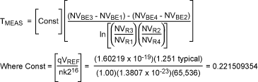
Equation 2. Simplified four-current temperature measurement equation.
Four-Current Method Example Using Real Data The temperature was measured on an evaluation (EV) kit at room temperature using the procedure above with the following results.
| For I1 | NVBE1 = 0x81AF | NVR1 = 0x0350 |
| For I2 | NVBE2 = 0x9048 | NVR2 = 0x32D4 |
| For I3 | NVBE3 = 0x90A5 | NVR3 = 0x3629 |
| For I4 | NVBE4 = 0x93E2 | NVR4 = 0x615c |
Using Equation 2 above and substituting the measured values:
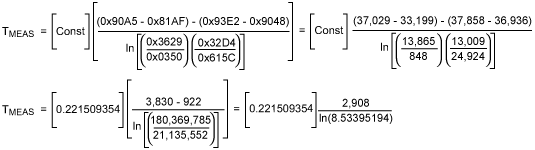
Solving the equation for the temperature yields: TMEAS = 300.19K
Converting the result from Kelvin to Celsius yields: ° C = 300.19-273.15 = 27.04 ° C
This is the measured value at room temperature. A correction for gain and offset has not been applied. The gain and offset correction is detailed below.
External Four-Current MethodThe external four-current method is the same as the internal four-current method, except that the internal current-source multiplexer must be changed to direct the current source out AIN1 or AIN2. The ADC input multiplexer must also be changed to use AIN1 and AIN2 as the ADC inputs.
The external components are connected as shown in Figure 1 above. The external transistor chosen for this application is a low-cost surface-mount 2N3904 from On SemiconductorSM, part number MMBT2N3904LT1. Other transistors or diodes can also be selected. The resistor chosen is a low-cost surface-mount 4.02K 1% size 0805 1/8 watt from Panasonic®, part number ERJ-6ENF4021V. This value resistor was chosen to match the internal resistor, which is typically 4KΩ.
Procedure Using the External TransistorThe procedure for measuring the voltages across the external transistor and external resistor is similar to the internal four-current method, except that the current source must be selected to drive AIN1 or AIN2 and different inputs must be selected to read the external VBE and VR.
Step 1. Enable the Reference and ADCEnable the internal 1.251V reference and the reference buffer with a gain of 1.0 by setting REFV [1: 0] bits to 0x01 in the REF_SDC register.
Enable the ADC by setting the ADCE bit in the ADC register. The internal reference and ADC are enabled. Note: The ADC is set with the default parameters of unipolar, normal polarity, single conversion, internal reference, unity gain, 10 samples per second , and normal conversion.
Step 2. Calibrate the ADCSet the ADC conversion mode to Self Offset and Gain Calibration by setting the Mode [2: 0] bits to 0x07 in the ADC register. Start an ADC conversion by setting the STRT bit in the ADC register. The ADC is now calibrated. The Mode [2: 0] bits in the ADC register are automatically cleared. This returns the ADC to normal operation.
Step 3. Set the Current Source for Internal AIN1Set the current source for internal temperature sensor by setting the IMUX [1: 0] bits to 0x10 in the TEMP_CTRL register.
Step 4. Set the Current Source for I1 (4µA) Set the current source for I1 by setting the IVAL [1: 0] bits to 0x00 in the TEMP_CTRL register.
Step 5. Set the ADC Input for AIN1 to AIN2 Set the ADC positive input multiplexer for AIN1 by setting MUXP [3: 0] to 0x00 in the MUX register. Set the ADC negative multiplexer for AIN2 by setting MUXN [3: 0] to 0x07 in the MUX register.
Step 6. Measure VBE1 Using the ADCThe VBE1 voltage is measured from the AIN1 to the AIN2 inputs to the ADC. The ADC is configured and only needs to convert to get the resulting VBE1 voltage. To start the ADC conversion, set the STRT bit in the ADC register. The ADC will do a conversion and the result will be in the DATA register. Read the DATA register value and save as a 16-bit integer named VBE1 for later calculation.
Step 7. Set the ADC Input for VR1 Set the ADC positive input multiplexer for AGND by setting MUXP [3: 0] to 0x09 in the MUX register. Set the ADC negative multiplexer for AIN2 by setting MUXN [3: 0] to 0x07 in the MUX register. To measure the AIN2 input relative to AGND, the polarity flipper bit is used. Set the POL bit in the ADC register. The ADC is now setup with AIN2 as its positive input and AGND as its negative input.
Step 8. Measure VR1 Using the ADCTo start the ADC conversion, set the STRT bit in the ADC register. The ADC will do a conversion and the result will be in the DATA register. Read the DATA register value and save as a 16-bit integer named VR1 for later calculation.
Step 9. Set the Current Source for I2 (60µA) Set the current source for I2 by setting the IVAL [1: 0] bits to 0x01 in the TEMP_CTRL register.
Step 10. Set the ADC Input for AIN1 to AIN2 Set the polarity flipper back to normal by clearing the POL bit in the ADC register. Set the ADC positive input multiplexer for AIN1 by setting MUXP [3: 0] to 0x00 in the MUX register. Set the ADC negative multiplexer for AIN2 by setting MUXN [3: 0] to 0x07 in the MUX register.
Step 11. Measure VBE2 Using the ADCThe VBE2 voltage is measured from the AIN1 to the AIN2 inputs to the ADC. The ADC is already configured and only needs to convert to get the resulting VBE2 voltage. To start the ADC conversion, set the STRT bit in the ADC register. The ADC will do a conversion and the result will be in the DATA register. Read the DATA register value and save as a 16-bit integer named VBE2 for later calculation.
Step 12. Set the ADC Input for VR2Set the ADC positive input multiplexer for AGND by setting MUXP [3: 0] to 0x09 in the MUX register. Set the ADC negative multiplexer for AIN2 by setting MUXN [3: 0] to 0x07 in the MUX register. To measure the AIN2 input relative to AGND, the polarity flipper bit is used. Set the POL bit in the ADC register. The ADC is now setup with AIN2 as its positive input and AGND as its negative input.
Step 13. Measure VR2 Using the ADCTo start the ADC conversion, set the STRT bit in the ADC register. The ADC will do a conversion and the result will be in the DATA register. Read the DATA register value and save as a 16-bit integer named VR2 for later calculation.
Step 14. Set the Current Source for I3 (64µA) Set the current source for I3 by setting the IVAL [1: 0] bits to 0x10 in the TEMP_CTRL register.
Step 15. Set the ADC Input for AIN1 to AIN2 Set the polarity flipper back to normal by clearing the POL bit in the ADC register. Set the ADC positive input multiplexer for AIN1 by setting MUXP [3: 0] to 0x00 in the MUX register. Set the ADC negative multiplexer for AIN2 by setting MUXN [3: 0] to 0x07 in the MUX register.
Step 16. Measure VBE3 Using the ADCThe VBE3 voltage is measured from the AIN1 to the AIN2 inputs to the ADC. The ADC is already configured and only needs to convert to get the resulting VBE3 voltage. To start the ADC conversion, set the STRT bit in the ADC register. The ADC will do a conversion and the result will be in the DATA register. Read the DATA register value and save as a 16-bit integer named VBE3 for later calculation.
Step 17. Set the ADC Input for VR3 Set the ADC positive input multiplexer for AGND by setting MUXP [3: 0] to 0x09 in the MUX register. Set the ADC negative multiplexer for AIN2 by setting MUXN [3: 0] to 0x07 in the MUX register. To measure the AIN2 input relative to AGND, the polarity flipper bit is used. Set the POL bit in the ADC register. The ADC is now setup with AIN2 as its positive input and AGND as its negative input.
Step 18. Measure VR3 Using the ADCTo start the ADC conversion, set the STRT bit in the ADC register. The ADC will do a conversion and the result will be in the DATA register. Read the DATA register value and save as a 16-bit integer named VR3 for later calculation.
Step 19. Set the Current Source for I4 (120µA) Set the current source for I4 by setting the IVAL [1: 0] bits to 0x11 in the TEMP_CTRL register.
Step 20. Set the ADC Input for TEMP + to TEMP-Set the polarity flipper back to normal by clearing the POL bit in the ADC register. Set the ADC positive input multiplexer for AIN1 by setting MUXP [3: 0] to 0x00 in the MUX register. Set the ADC negative multiplexer for AIN2 by setting MUXN [3: 0] to 0x07 in the MUX register.
Step 21. Measure VBE4 Using the ADCThe VBE4 voltage is measured from the AIN1 to the AIN2 inputs to the ADC. The ADC is already configured and only needs to convert to get the resulting VBE4 voltage. To start the ADC conversion, set the STRT bit in the ADC register. The ADC will do a conversion and the result will be in the DATA register. Read the DATA register value and save as a 16-bit integer named VBE4 for later calculation.
Step 22. Set the ADC Input for VR4Set the ADC positive input multiplexer for AGND by setting MUXP [3: 0] to 0x09 in the MUX register. Set the ADC negative multiplexer for AIN2 by setting MUXN [3: 0] to 0x07 in the MUX register. To measure the AIN2 input relative to AGND, the polarity flipper bit is used. Set the POL bit in the ADC register. The ADC is now setup with AIN2 as its positive input and AGND as its negative input.
Step 23. Measure VR4 Using the ADCTo start the ADC conversion, set the STRT bit in the ADC register. The ADC will do a conversion and the result will be in the DATA register. Read the DATA register value and save as a 16-bit integer named VR4 for later calculation.
Step 24. Calculate the TemperatureThe temperature calculation is identical to the four-current internal method. Use that method with the eight saved measurements to calculate the external temperature.
Gain and Offset CorrectionThe TEMP_CAL register is provided to correct for gain and offset errors in the temperature-measurement circuit. To correct for the gain and offset errors, the following formula is used.
TACTUAL = g (TMEAS) + TOFFSET
Equation 3. Gain and offset correction equation.
Procedure for Gain and Offset CorrectionThe procedure for adding the gain and offset correction is detailed below. The procedure reads the values ​​from the gain and offset correction registers. The gain and offset amounts are then computed using two formulas. The resulting correction values ​​are applied to Equation 3 above.
Step 1. Measure and Calculate the TemperatureUse the procedure for the internal or the external transistor and save the result as TMEAS for use in the correction formula above.
Step 2. Read the TGAIN RegisterRead the TEMP_CAL register and save the upper byte TGAIN [7: 0] for use in the formula below. It should be saved as a type-signed integer.
Step 3. Calculate the Gain Correction FactorUsing the value saved above, apply this value to the gain formula below.
Gain = 0.9025 + TGAIN × 0.000576
Equation 4. Gain formula equation.
Step 4. Read the TOFFS RegisterRead the TEMP_CAL register and save the lower byte TOFFS [5: 0] for use in the formula below. The data should be saved as a type-signed integer. Do not right-shift the data.
Step 5. Calculate the Offset Correction FactorUsing the offset value saved above, apply this value to the gain formula below.
Offset = -14.0 + TOFFS × 0.3125
Equation 5. Offset correction equation.
Step 6. Calculate the Corrected TemperatureUse the gain and offset values ​​calculated above in the temperature equation below.
TACTUAL = GAIN × TMEAS + OFFSET
ConclusionThe MAX1358 features internal circuitry to measure the internal die temperature. The internal circuitry can also be used with an external transistor for a low-cost remote temperature sensor. The four-current temperature measurement method described in this application note can be used to achieve the ± 0.5 and ± 1.0 typical accuracy specified in the MAX1358 data sheet.
On Semiconductor is a registered service mark of Semiconductor Components Industries, LLC.
Panasonic is a registered trademark of Matsushita Electric Industrial Co., Ltd.
In order to meet customer commercial use, we developed and strongly recommend our 5.5inch PDA Handheld Terminal. With its stylish and fashionable appearance, it gains popularity in market. It is not only a Barcode Scanner PDA with built in printer, but also can support expand functions such as UHF reader, Fingerprint scanner, IC card reader and etc. Welcome to contact us for more information!

5.5inch PDA Handheld Terminal
Pda Rfid Scanner,Pda With Fingerprint Scanner,Pda With Built In Scanner,Android Handheld Terminal With Printer
Shenzhen Qunsuo Technology Co., Ltd , https://www.qsprinter.com