MAX14921: PCB Layout Guide for 12/16-Battery High-Precision Measurement Analog Front Ends
Introduction
The MAX14921 is a high-performance, high-accuracy battery pack measurement circuit. The improvement in measurement accuracy is especially important for new lithium iron phosphate batteries because the charge and discharge curves of such batteries are very flat, especially at a state of charge (SOC) of 65% to 95% full charge. The excellent accuracy stems from the MAX14921's unique sample/hold architecture, which minimizes battery voltage sampling errors and errors in sampling at different stages of the battery.
High-precision features also depend on careful circuit design. This article introduces some simple and effective layout principles to help you get the best accuracy.
Reduce noise
The following noise-related design guidelines have become very popular in modern PCB layouts. This article presents layout considerations for noise suppression in the MAX14921.
Bypass capacitor
Bypass capacitors are important circuit components, and integrated circuits (ICs) operate normally based on good noise filtering. For best performance, the bypass capacitor should be placed as close as possible to the IC's power supply pins. Table 1 lists the bypass capacitor requirements for the MAX14921.
Table 1. MAX14921 Bypass Capacitor Requirements 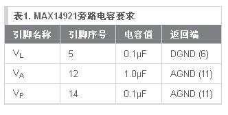
The capacitor can be mounted on the left side of the IC. This area contains the digital SPI interface, analog input for T1/T2/T3, analog output, power supply pins, and some sampling capacitors. To alleviate the crapped layout space, you can use the back area of ​​the MAX14921. You can use the via connection signal of the PCB solder layer under the MAX14921 and the capacitance of this area.
Keep the distance between the holding capacitor and the corresponding power supply pin as short as possible. For some layouts, you can place the capacitor on the back of the board. If there is only one bypass capacitor, place it next to the device, such as the 12th foot (VA) capacitor.
Taking a 4-layer board as an example, some layout examples are listed below. In these examples, the top trace is red, the second layer is DGND (green), the third layer is V5V (yellow), and the fourth layer is the bottom trace (blue). First understand the bypass of VL, assuming VL is 3.3V. In Figure 1, connect the 5th pin to the back of the board through the via and the bypass capacitor C22 on the back of the board (below the MAX14921). The other pin of the capacitor is connected to the second layer of the PCB through the via, DGND.
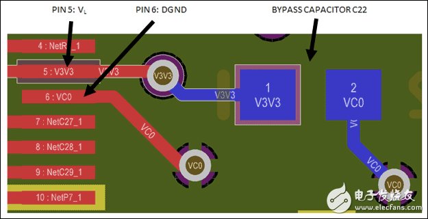
Figure 1. Example of the MAX14921 5th pin bypass capacitor.
Figure 2 shows how to connect the VP bypass. In the case of pin5, the pin of the IC is connected through a via and a bypass capacitor placed on the back. Since the return pin of the 13th pin is AGND, the other end of C24 is connected to the 11th pin instead of the DGND plane.
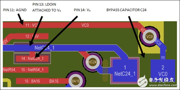
Figure 2. MAX14921 pin 14 bypass capacitor layout.
The connection of the VA bypass capacitor can be seen from Figure 3. Follow the instructions below to lay the AGND (10th pin) signal line in parallel with the AOUT (10th pin) signal line. Based on this consideration, it is usually easier to place the 12th pin bypass capacitor on the same side of the MAX14921 PCB, making full use of the bypass capacitor.
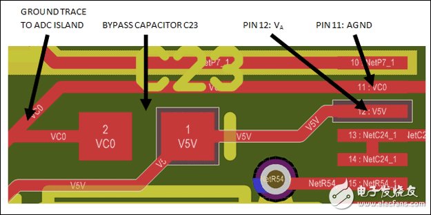
Figure 3. The bypass capacitor connection for pin 12 of the MAX14921.
ADC wiring isolation
Another technique for noise management is to provide a separate ground plane below the sensitive analog components. Figure 4 shows an example of an independent ground plane for the ADC, connecting U3 and pin 11 to this ground plane. The white silkscreen box highlights the vias from the left bypass capacitor C20 that connect the AGND of the MAX14921 to the separate ground plane of the ADC, which is dedicated to this separate ground plane. The only connection point between DGND and the AGND plane is located at the top right of the ADC's independent ground plane and is indicated by a white silkscreen frame.
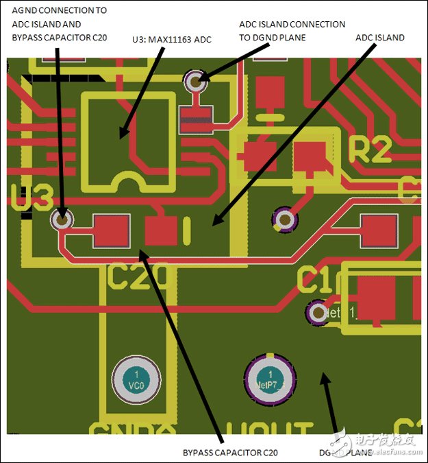
Figure 4. Ground plane isolation from the ADC (U3).
Dog Training Receiver,Waterproof Dog Shock Collar,Rechargeable Remote Dog Trainer,Small Dog Shock Collar With Remote
Elite-tek Electronics Ltd , https://www.aetertek.ca