A practical design of vehicle inverter
With the improvement of the economic level, cars are gradually becoming the daily means of transportation for people. However, electronic products that people carry with them, such as mobile phones, cannot use the power supply in the car. Therefore, the development of a cost-effective car inverter has become a demand. We use the integrated pulse width modulation chip SG3525A as the main control chip, and the CD4020B counter and the NAND gate circuit form a frequency division and phase separation circuit and are equipped with a protection circuit to realize the pulse width modulation of the inverter. The continuous output power of the inverter power supply is 100W, and has the functions of output overcurrent protection and input undervoltage protection, which can realize power inverter, voltage stability, undervoltage protection and overcurrent protection.
This article refers to the address: http://
Basic principle of the system
The input end of the inverter is a car battery (+12V, 4.5Ah), and the output end is a power frequency square wave voltage (50Hz, 220V). The main circuit and control circuit block diagram of the system is shown in Figure 1. The typical two-stage transformation, DC/DC conversion and DC/AC inverter, is adopted. The 12V DC voltage is inverted into a high-frequency square wave by push-pull conversion, boosted by a high-frequency step-up transformer, and then rectified and filtered to obtain a stable DC voltage of about 320V; then, by bridge conversion, square wave inverter will be used. The stable DC voltage is inverted into a square wave voltage with an effective value slightly larger than 220V to drive the load. In order to ensure the reliable operation of the system, DC high-voltage side voltage signal, current signal and battery voltage signal are respectively collected and sent to SG3525A to realize voltage regulation, over-current protection and under-voltage by adjusting the duty cycle or shutdown pulse of the drive pulse. Protection and other functions.
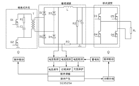
Figure 1 System main circuit and control circuit block diagram
The main technical parameters
Input voltage: DC 12V;
Output voltage: AC 220V ± 5%, 50Hz ± 2%;
Rated power: 100W;
Protection function: input DC polarity reverse protection, input undervoltage protection, output overcurrent protection.
Circuit design
1 main control chip SG3525A
The SG3525A is a pulse width modulator control IC manufactured by ST. It has integrated reference voltage, oscillator synchronization, soft start time control, and input under voltage lockout. The pins of the SG3525A are shown in Figure 2.
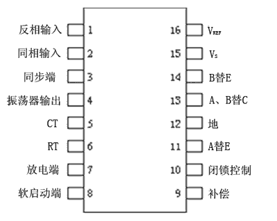
Figure 2 SG3525A pin distribution
Determination of the oscillation frequency: The oscillation frequency is set by three external components RT, CT and RD, which are connected to the 6, 5, and 7 pins, respectively. The oscillation frequency is fOSC=1/CT(0.7RT +3RD), where 0.7RTCT is the timing capacitor charging time and 3RDCT is the timing capacitor discharging time. In order to make the frequency division and phase separation circuit obtain the 50Hz oscillation frequency, the design sets the oscillation frequency to 51.2kHz, taking CT=2000pF, RT=10kΩ, and RD=922Ω.
Output Pulse Width Adjustment: The PWM pulse width is controlled by the lower level of pins 9 and 8. The error amplifier U1 inside the chip amplifies the voltage feedback signal and the reference voltage signal and sends it to the inverting input terminal of the comparator U2. The input of the comparator positive input terminal is from the sawtooth wave on the capacitor CT, and the two are compared and output. The square wave pulse controls the duty cycle of the SG3525A's internal output power amplifier tube (see Figure 3). In this design, the 8-pin is grounded via a capacitor, and the 9-pin is connected to the feedback voltage of the DC/DC high-voltage DC voltage, thereby adjusting the stability of the output DC voltage. In Figure 3, U1 is the error amplifier in SG3525A, 1, 2, and 9 are chip pins, respectively, and R1 to R7, C1, and C2 are external resistors and capacitors. The SG3525A's 16-pin output 5V reference voltage. Resistors R3, R4 and U1 form an inverse proportional operator, R4/R3 is its static amplification factor, and the larger the value, the higher the control accuracy. However, if the amplification is too large, it will cause oscillation. Therefore, the introduction of C1 and R5 makes the error amplifier an incomplete proportional integral controller. At this time, the static error amplification factor is constant, and the dynamic error amplification factor is reduced, which does not affect the control accuracy and avoids overshoot. Causes oscillation.
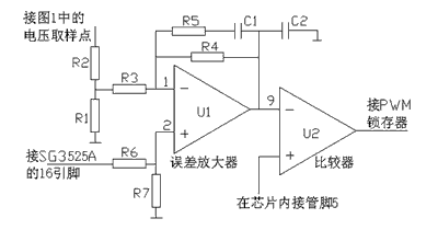
Figure 3 Output DC high voltage regulation schematic
Pulse off: When the 10 pin is high, the output pulse is blocked. This design uses this function to protect the output overcurrent and overvoltage and input undervoltage.
2 frequency division and phase separation circuit
The frequency division circuit is composed of a 14-stage serial binary counter/distributor CD4020B, and the frequency division signal is from the oscillator output terminal 4 of the SG3525A. A, B, and C in Fig. 4 represent the waveforms of the oscillator pulses divided by 8, 9, and 10, respectively, and their frequencies are fA=fOSC/28, fB=fOSC/29, and fC=fOSC/210, respectively. The split-phase circuit consists of a single-chip two-input four-NAND gate CD4011BC and peripheral devices, which combines the signal ABC logic into the drive pulse (A+B)C and (A+B)C signals required by the inverter bridge. The drive signal has a common dead band with a signal frequency of approximately 50 Hz.
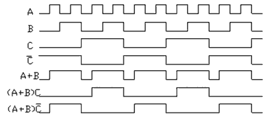
Figure 4 frequency division and phase separation waveform
3 protection circuit
1 input undervoltage protection
As shown in Figure 5, D1 is the battery polarity reverse connection protection. Pin 16 of SG3525A outputs a reference voltage of 5V, taking R3=R4=10kΩ. Under normal conditions, the inverting input voltage of U1 is greater than the voltage of the forward input terminal, U1 outputs a low level, and diodes D1 and D2 are turned off. When the battery voltage is lower than 10V, the comparator U1 starts to work, the output changes from low level to high level, D2 and D3 are turned on, and the potential of the non-inverting input terminal is raised to a high level, so that U1 is always stable and output high power. Flat, output a shutdown signal to pin 10 of the SG3525A.
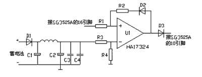
Figure 5 Input undervoltage protection circuit
2 output current overload protection
As shown in Figure 6, the op amp U2 and the peripheral resistors form an inverse proportional amplifier, and the op amp U3 and peripheral circuits form a comparator. R3 in Figure 1 is the sampling resistor, taking 2.2Ω, 2W. When the load current increases, the voltage drop ΔU of the resistor increases.
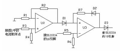
Figure 6 output current overload protection circuit
The input voltage of the forward input terminal of the operational amplifier U3 is: U+=(1+R2/R1)×(R3/R4)×△U
Reasonably adjust the values ​​of R1, R2, R3, and R4 so that when the load current exceeds 1.5A, the potential of the forward input terminal of U3 is higher than the reverse input terminal, the output is high, and the diodes D2 and D3 are turned on. The potential of the non-inverting input is raised to a high level, so that U1 always outputs a high level and outputs a shutdown signal to the 10 pins of the SG3525A.
Thermal design
In order to further reduce the volume and reduce the weight, a heat dissipation method using the outer casing (the casing) is adopted, which not only solves the heat dissipation, but also reduces the volume of the whole machine and reduces the weight.
Inverter test output waveform
The DC/DC converter output voltage is stable at 320V, and the inverter bridge switching frequency is 50Hz, which is connected to a 500Ω resistor load. The circuit waveform of the experiment is shown in Figure 7.
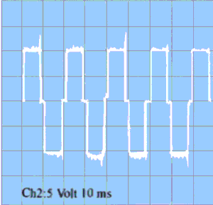
Figure 7 test circuit output waveform
Conclusion
The vehicle-mounted inverter power supply circuit designed in this paper mainly adopts integrated chip, which makes the circuit structure simple, stable performance and low cost. The actual application proves that the inverter power supply works stably and reliably, and can continuously output power of 100W.
Flip Desk Clock,Small Desk Clock With Light,Table Clock Font With Light,Table Clock Modern
Guangzhou Huanyu Clocking Technologies Co., Ltd. , https://www.findclock.com