Wireless USB control system based on nRF24L01
Today, wireless technology is rapidly developing, and the field of application is becoming wider and wider. Compared with wired technology, wireless technology has the advantages of convenience, flexibility, reduced wiring construction difficulty, and reduced cost. This paper describes the composition, function and design method of wireless USB control system. The system consists of PC, wireless USB controller and multiple terminal nodes. This paper presents a scheme for implementing wireless USB controller and terminal node: Wireless USB The controller's solution is based on the microcontroller STC89C58RD+ as the microcontroller, based on Nordic's 2.4GHz wireless transceiver chip nRF24L01, combined with Philips' PDISUBD120D USB control chip; the terminal node solution is based on STC89C58RD+ microcontroller, based on The nRF24L01 wireless transceiver chip is implemented according to the actual application circuit required.
1 system composition and its implementation1.1 System Description
As shown in FIG. 1, the composition of the wireless USB control system includes a PC, a wireless USB controller, and terminal nodes (n). The PC and the wireless USB controller communicate through the USB interface. On the PC side, the VC++ development application is used to control the wireless USB controller, and the wireless USB controller and each terminal node implement wireless communication through the wireless transceiver chip nRF24L01.

1.2 system implementation
1.2.1 Wireless USB Controller Implementation Solution
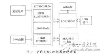
The wireless USB controller implementation scheme is shown in Figure 2. It mainly includes the microcontroller STC89C58RD+, the USB control chip PDIUSBD12, and the wireless module nRF24L01 Module. The STC89C58RD+ contains 32KB of program memory, 1280B RAM and 16KB E2PROM. E2PROM can be used to store the address of the terminal node and other data that needs to be stored in power down. The 32KB program memory and 1280B RAM can meet most application requirements. The USB control chip PDIUSBD12 is a performance-optimized USB control device that is fully compliant with the USB 1.1 specification and supports local DMA transfers for microcontroller-based systems. The maximum supported transmission speed of USB1.1 is 12Mb/s, which is faster than the average PC interface, which is enough for the application of wireless USB control system. The wireless module uses Nordic's nRF24L01 single-chip RF transceiver chip. The chip operates in the ISM (Industrial, Medical, and Scientific) band of 2.400~2.4835GHz, and operates at 1.9~3.6V. There are up to 126 channels to choose from. Support multi-point communication, the maximum rate is up to 2Mb/s, built-in link layer, which reduces the complexity and cost of MCU, improves the reliability of data transmission, and only needs a small number of peripheral components to form RF transceiver circuit. It has the advantages of small size, low power consumption and high cost performance.
1.2.2 terminal node implementation scheme
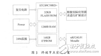
The terminal node implementation scheme is shown in Figure 3. It mainly includes the microcontroller STC89C58RD+, the wireless module nRF24L01 Module, and the expansion circuit of the actual application requirements. The STC89C58RD+ microcontroller and the nRF24L01 wireless module form the basis of wireless communication between the terminal node and the wireless USB controller. The extension circuit of the terminal node is designed according to the actual application requirements. For example, when applied to a temperature data acquisition system, the expansion circuit should be The temperature sensor circuit and the flexible setting of the terminal nodes enable the entire system to meet the needs of a variety of applications.
2.1 nRF24L01 wireless module schematic
nRF24L01 is a single-chip RF transceiver chip from Norway's Nordic VLSI. It is available in 20-pin 4mm & TImes; 4mm QFN package. It has built-in frequency synthesizer, power amplifier, crystal oscillator, modulator and other functional modules. It uses Enhanced ShockBurst technology and uses SPI interface. Communicate with the microcontroller, the speed is 0~8Mb/s, and the configuration is convenient. The nRF24L01 is ideal for wireless data communications, wireless PC peripherals, wireless alarm and security systems, wireless unlocking, wireless monitoring, home automation and toys. Please refer to the reference for the specific functions and working modes of the chip and its programming process. The circuit schematic of the module is shown in Figure 4.
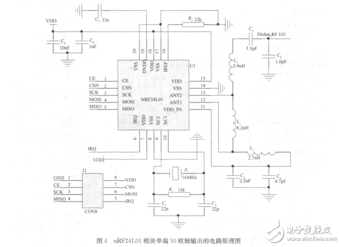
The nRF24L01 module uses double-panel for PCB layout. The bottom layer is all grounded, and the top layer is placed with components. All capacitors and resistors are made with 0402 package capacitors and inductors as close as possible to the chip pins. The top layer also needs to be laid over a large area, and a large number of layers are placed on the top and bottom layers. Through hole. The module supply voltage is 3.3V, the SPI interface can be directly connected to the IO port of the 5V MCU, and the MCU without SPI interface can use the IO port to simulate the SPI timing, which is convenient to use.
2.2 USB control chip PDIUSBD12 schematic
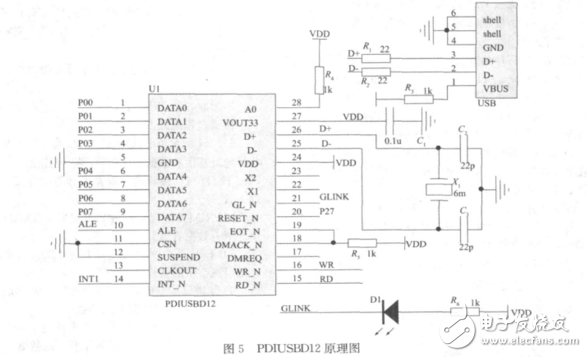
The PDIUSBD12 is a high-priced USB control chip that works with the MCU. This gives the designer the flexibility to select the MCU, which communicates with the MCU via a parallel interface and also supports local DMA transfers. Figure 5 is a schematic diagram of the connection between PDIUSBD12 and STC89C58RD+ microcontroller.
The above figure does not show the STC89C58RD+ MCU. Only the dot names are given. For example, P00-P07, P27, ALE, INT1, WR, RD, STC89C58RD+ is fully compatible with the standard 80C51 (such as AT89S51) pin. The connection between PDIUSBD12 and MCU is 2 ways: bus mode and separate address data mode. When using the bus mode, the ALE of pin 10 is connected to the ALE of the MCU, and the A0 of the pin 28 is connected to the high level; when the address data is separated, the ALE is connected to the low level, and the A0 is connected to any IO port, data or address ( Command) is distinguished by A0. Figure 5 uses the bus method. In addition, the wireless USB controller directly uses the USB interface to supply power, eliminating the need for power and reducing costs.
High Speed Blender,Ipl Laser Hair Removal,Diy Laser Hair Removal,Best Ipl Hair Removal,Epilator Ipl
SHENZHEN CHONDEKUAI TECHNOLOGY CO.LTD , https://www.szfourinone.com