Design principle of intelligent all-digital special frequency converter
1 Introduction
This article refers to the address: http://
The medical treatment device is a person, which determines the strictness of the requirements of its transmission control system, especially for the treatment of cervical spondylosis and lumbar disc herniation, and proposes the safety and accuracy of the transmission system. Higher requirements: stalling is absolutely not allowed, offside is not allowed, and parking is accurate. At the same time, in order to simplify the design of the mechanical part and reduce the related sensors, most of the control functions are electrically controlled by the principle of mechatronics.
The therapeutic device transmission system requires the motor speed to be controlled between 100 and 250 r/min, and then decelerated by a 50:1 mechanical reducer with a transmission torque of >1.5 Nm. The amplitude of the swing is required to be cervical vertebra: ±30° to ±60°; lumbar vertebra: ±60° to ±100°; the starting point should be controlled at the center position. The speed and swing should be adjustable according to the specific case.
2Intelligent design of all-digital dedicated inverter
(1) Taking into account the special requirements of medical therapeutic instruments, in order to improve the operational reliability and control accuracy of the frequency converter, intelligent digital design is adopted, and also combined with the characteristics of miniaturization, the main power device adopts the IGBT intelligent power module of Mitsubishi Electric of Japan. (IPM) PM20CSJ060. The input is single-phase 220V AC, and is supplied to the intelligent power module after being rectified by the single-phase full-bridge rectifier. The output is three-phase 220V AC, and the 0.5kW three-phase asynchronous motor is connected to the â–³ connection method.
(2) Using INTEL's 16-bit single-chip 80C196KC as the system CPU, it has the characteristics of fast computing speed, high precision and strong command function. With 8 10-bit A/D converters, it can detect analog and digital signals. Control calculation and data processing, logic judgment of protection function, send setting and control data to PWM generation circuit SA4828, and manage functions such as keyboard and digital display.
(3) The SPWM wave generator adopts the enhanced motion control large-scale integrated circuit SA4828 from MITEL of the United Kingdom. The chip works as a microprocessor-independent peripheral, but it can be controlled by any type of microprocessor with little or no additional logic. The pin configuration makes it suitable for most bus formats, including multiplexed address/data bus formats and RD/WR or R/W control modes. Since the intervention of the microprocessor is required only when the operating state is changed, the chip hardly occupies the resources of the CPU during operation.
The SA4828 is fully digital and operates at carrier frequencies up to 24 kHz. There are three optional output power waveforms in the internal ROM, and harmonic suppression technology reduces power device losses. 16-bit frequency control accuracy, three independent amplitude registers for three-phase unbalance compensation. The hardware structure of the inverter designed with SA4828 is shown in Figure 1.

Figure 1 shows the hardware structure of the inverter using SA4828
3SA4828 features and working principle
3.1SA4828 pin diagram and pin function description
The pin diagram of SA4828 is shown in Figure 2. The pin function description is shown in Table 1.
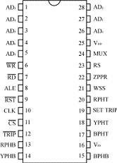
Figure 2 SA4828 pin diagram
Table 1 SA4828 pin description

3.2 SA4828 internal structure block diagram and working principle
Figure 3 is a block diagram of the internal structure of the SA4828. It can be seen from the figure that the SA4828 is mainly composed of three parts:
(1) Receive and store the microprocessor command (control word) part, which is mainly controlled by bus, bus decoding, register R0, R1...R5, virtual register R14, R15 and 32-bit initialization register and 48-bit control Register composition;
(2) reading a portion of the modulated waveform from the waveform ROMS, which is composed of an address generator and a waveform decompression buffer;
(3) Three-phase output control circuit and output pulse latch circuit, each phase output control circuit is composed of pulse deletion circuit and pulse delay circuit.
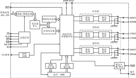
Figure 3 internal block diagram of the SA4828 chip
The SA4828 chip has a parallel interface to communicate with the microprocessor. This interface is compatible with almost all industry standard microprocessors such as 8051, 0096, 6805, 68000 and TMS320 without regard to the width of the bus and the addition of additional logic. Most data bus structures can be divided into a multiplexed address/data bus and a separate address/data bus, while most microprocessors are not WR/RD structures or R/W structures; and the chip is designed to work with the above four Any combination of the combinations is used. All bus formats are distinguished by the status of one configuration pin (MUX) and one register select pin (RS).
More importantly, in the case of system anomalies (overcurrent or overvoltage), an emergency shutdown input (SETTRIP) can quickly shut down all PWM outputs without the control of the microprocessor, which is a good solution to the frequency conversion. The fast protection of the device avoids the delay caused by the CPU interrupt service instruction cycle.
3.3SA4828 chip control function
Control of the SA4828 chip is achieved by the microprocessor interface sending data to the internal two registers. They are initialization registers and control registers.
The initialization registers are used to set some basic parameters related to the motor and inverter. These parameters are initialized before the motor is operated and are generally not allowed to change when the motor is operating.
The control register controls the state of the pulse width modulated wave during motor operation to further control the operation of the motor, such as speed, forward/reverse, start and stop. The contents of the registers are often rewritten during motor operation to achieve real-time control of the motor.
Due to the limitation of the 8-bit data interface, the data must first be read into six temporary registers R0, R1...R5, which are then sent to the corresponding initialization or control registers. The new data can only really work when it is written to the corresponding register.
The transfer of data is accomplished by the operation of writing to a virtual register. For example, the write register R14 transfers the initialization data to the initialization register, and the write register R15 transfers the control data to the control register. Since R14 and R15 are not actual registers, it does not matter what data is written. The operation of writing data here actually performs the operation of transferring data to the initialization register or the control register.
(1) Initialization register programming
The initialization register will determine the following parameters: carrier frequency, power frequency range, pulse delay time, pulse cancellation time, waveform selection, development amplitude control of the special inverter for medical therapy instrument, counter reset (this function can make the SA4828 internal modulation frequency counter Set to 0, this time disable normal frequency control operation, each phase output duty cycle is 50% pulse), software reset, etc. These parameters are determined by the corresponding control words that are sent to the four 8-bit registers R0, R1, R2, and R3 before being sent to the 32-bit initialization register. Its contents are shown in Table 2:
Table 2 Register contents
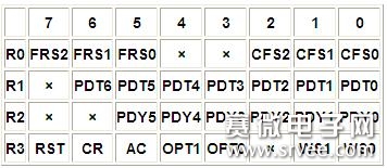
Note: The unused bits (×) should be written to 0, which is compatible with future products.
1 carrier frequency selection
The CFS word in R0 is called the carrier frequency selection word. Let n be the decimal number corresponding to the CFS word. The actual carrier frequency fc is: fc= 
Where fk is the external clock frequency.
2 output power frequency range selection
The FRS word in R0 is called the power frequency range selection word. Let m be the decimal number corresponding to the FRS word. The actual output power frequency fr is: fr= 
3 pulse delay time selection
The PDY word in R2 is the pulse delay time selection word, and x is the decimal value corresponding to the PDY word. The actual pulse delay time Tpdy is determined by the following formula: Tpdy= 
4 pulse cancellation time selection
The PDT word in R1 is the pulse cancellation time selection word, and y is the decimal value corresponding to the PDT word. The actual pulse cancellation time Tpdt is determined by the following formula: Tpdt= 
It should be noted that since the pulse delay circuit follows the pulse-removal circuit (see Figure 3), the actual minimum width of the output PWM pulse will be narrower than the set pulse cancellation time. The actual minimum pulse width is Tpdt. Tpdy.
5 waveform selection
The two bits of WS1 and WS0 in R3 are used to determine the power waveform of the output. See Table 3 for details. The waveform can be represented by a specific mathematical expression, and the specific shape is shown in FIG.
Table 3 WS1, WSO determined output power waveform
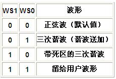

Figure 4 SA4828 internal modulation waveform
(a) sine wave (b) fundamental wave plus third harmonic (c) fundamental wave with dead zone plus third harmonic
6 amplitude control (AC)
The amplitude control bit (AC) in R3 defines the controlled mode of the three-phase waveform amplitude. When AC=0 (chip default), the red phase amplitude in the control register is used to control the amplitude of all three-phase modulation frequencies. When AC=1, three independent amplitude registers are used to control the amplitude of the corresponding phase modulation frequency.
7 counter reset (CR)
When the counter in R3 resets CR=1, the red phase phase counter is set to 0. At this time, the normal frequency control operation is prohibited, and the output duty cycle of each phase is 50%.
8 software reset (RST)
When RST=1 in R3, the entire chip is reset to the initial state of initialization, and its effect is equivalent to the hardware reset pin RST.
(2) Programming of control registers
The control register is a 48-bit register. The data of the control register is read into the temporary registers R0 to R5 in units of 8 bits, and then the data in R0 to R5 is transferred to the control register by writing the virtual register R15. The contents are shown in Table 4.
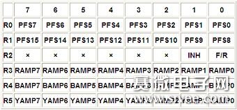
1 power frequency selection
The output supply frequency is linearly adjustable over the maximum supply frequency range. It is determined by a 16-bit power frequency selection word "PFS" and the entire supply frequency range is divided into 65536 equal parts. Since the PFS word spans two temporary registers R0, R1, when changing the output power frequency, the values ​​of the two temporary registers must be refreshed before the virtual register R15 is written.
The power frequency fp is determined by:  Fp=Pfs
Where: Pfs is the decimal value of the 16-bit PFS selection word.
2 power supply amplitude selection
The magnitude of the output supply is proportional to the sampled value in the internal ROM and the value of the 8-bit amplitude select word (RAMP, BAMP, YAMP). The percentage of the amplitude is calculated as follows:  APOWER=100%
Where: A is the decimal value of the 8-bit amplitude selection word.
It is worth noting that the amplitude control bit (AC) in the initialization register determines whether the value of the red phase amplitude register is used to control all three-phase output amplitudes.
3 positive / reverse selection
The phase of the three-phase PWM output is determined by the F/R selection bit in R2:
F/R=0 positive phase sequence is red-yellow-blue;
The F/R=1 reverse phase sequence is blue-yellow-red.
The output waveform remains continuous during forward and reverse switching.
4 output prohibition selection
When the output disable bit (INH) in R2 is active (1), all PWM outputs go low, and other operations inside the chip are not affected. When this bit is released, all the outputs are immediately restored.
It should be noted that the output disable circuit is after the pulse deletion and pulse width delay circuits, so some excessively narrow pulses may be generated at the beginning of the output inhibition.
3.4SA4828 chip programming example
The inverter of this example uses a 12.288MHz clock. The specific parameters of the initialization register design are as follows:
Carrier frequency 3kHz
Power frequency 15Hz
Pulse cancellation time 10μs
Pulse width delay time 5μs
The power waveform suppresses the waveform of the third harmonic
Amplitude control three-phase amplitude symmetry
(1) Initialization register programming example
1 set the carrier frequency by fc= 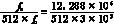 Got 2n=
  =8
=8
Then the CFS word in n=3R0 is 011H
2 set the output power frequency range from fr = 2m  Got 2m=
  =2
=2
Then m=1, and the FRS word in R0 is 001H.
3 set the pulse width delay time by Tpdy=  =5μs
=5μs
Available x=64- (Tpdy×fc×512)=56.32
Take the integer 56, then the 6-bit PDY word in R2 is 111000H
4 set the pulse cancellation time
Since the minimum pulse width of the actual output PWM pulse is Tpdt-Tpdy, the pulse width delay time should be added when setting the minimum pulse cancellation time.
Therefore, in this case the actual minimum pulse width should be 10μs + 5μs = 15μs by Tpdt = 
Available y=128- (Tpdt×fc×512)
=128-(15.2×10-6×3×103×512)
≈104.65
Taking the integer 104, the PDT value in R1 is 01101000H.
5 set waveform selection, amplitude control, etc.
The output waveform is selected as the fundamental wave plus the third harmonic, so WS1=0, WS0=1, no user output selection, so OPT1=0, OPTO="0". Set amplitude control bit AC=0, select three-phase balance amplitude control mode, counter reset and software reset are invalid during normal operation, so CR="RST"=0. So the binary code in R3 is 00000001. In summary, in the initialization register:
R0=0010001123H
R1=0110100068H
R2=0011100038H
R3=0000000101H
(2) Control register programming example
According to the specific requirements of the therapeutic device control, the inverter output frequency does not exceed 10 Hz, and the corresponding motor speed is 280 r/min. Since the output frequency needs to be adjusted at any time, use the analog input channel CH0 of the 80C196KC microcontroller to input the voltage signal provided by the 5.1kΩ resistor and the 10kΩ potentiometer to divide the +5V supply voltage. The analog quantity of the 80C196KC is converted to 10-bit precision, and the highest voltage supplied to the voltage divider is about 3.3V, and the sampling code is 680. Since the output power frequency accuracy of the SA4828 is 16 bits, the 10-bit sample value must be shifted to the left by 6 bits, then the low bit is sent to the temporary register R0, and the high bit is sent to R1.
Due to the VVVF control, the amplitude is proportional to the power supply frequency, and the sample value of the frequency setting potentiometer can be obtained, A×15/50, and then shifted to the right by 2 bits and then sent to the temporary register R3. Due to the three-phase balance amplitude, R4 and R5 can be assigned no value.
The output prohibition is invalid, so INH=0, the positive and negative F/R is changed periodically, the half-swing is started to rotate forward, F/R=0, so R2=0, and each time you want to change direction, R2 The D0 bit can be reversed.
The swing control can be realized by dividing the +5V power supply voltage into a 80C196KC analog input channel CH1 through a 10kΩ potentiometer.
4 treatment device control function realization
4.1 stall control
By setting the highest modulation frequency of the SA4828 to 10Hz, the speed is 280r/min, slightly higher than 250r/min, leaving a certain adjustment margin.
4.2 swing control
When the motor rotates at the maximum speed of 250r/min, after 1/50 of the reducer, the speed is 5r/min=1800°/min=30°/s. 100 ° / (30 ° / s) = 3.33 s. 200 ° / (30 ° / s) = 6.67 s. If 100ms is used as the control period, the full swing period T is: T=67× 
Where: t is the swing input sample value;
f is the speed input sample value.
The first swing at the beginning should start from the middle, so T1 = T/2. After the above processing, the position control is changed into the timing time control, which not only saves the position switch which is difficult to adjust, but also makes the control of the rotation speed and the swing width much more convenient. Quick and easy control is achieved with two potentiometers. When parking, the operator can accurately stop by pressing the turn/stop switch when going to the center position according to the visual inspection, and each time it rotates, it will rotate halfway from the center position, and then run back and forth in full amplitude. Since the 048 dc power is realized by the SA4828, accurate parking is achieved, and the regenerative energy generated by the motor braking is not fed back to the polar capacitance of the DC link, thereby avoiding the pumping voltage.
5 Conclusion
(1) The inverter designed by SA4828 has simple interface, strong function, high control precision and convenient use. It can constitute a high-performance variable frequency speed control system. SA series PWM controller has a good application prospect in the field of frequency conversion speed regulation.
(2) 16-bit single-chip control improves the intelligence of the system, the control speed is fast, the system performance is changed easily, and the functions of control, protection and human-machine interface are strong.
(3) Through the practical application on the medical treatment instrument, the frequency conversion control system works safely and reliably, the frequency control accuracy and stability are high, the output harmonic content is small, the low speed operation characteristics are good, the starting torque is large, and the parking is accurate and rapid. Speed ​​and swing adjustment is extremely convenient. As a special inverter design for special applications, it has the promotion value.
Flexible Glass Screen Protector
Flexible Glass Screen Protector,Screen Protector,Iphone Screen Protector,Full Size Screen Protector
Guangzhou Ehang Electronic Co., Ltd. , https://www.ehangmobile.com