Design of optical fiber transmission system for high speed video signals
The video signal with high frame rate is different from the ordinary video signal. If it is transmitted by analog signal, its analog bandwidth reaches tens of megabytes or even one or two hundred megabits, which makes it difficult to achieve long-distance transmission. The optical fiber transmission capacity is large, the quality is high, and it is not easily interfered. It is widely used in high-speed digital transmission systems. At present, there are quite a few optical fiber transmission systems for ordinary video signals at home and abroad, and there are few reports on non-standard high frame rate video signal fiber transmission systems, especially for single fiber transmission of two or more high frame rate video. No reports have been reported.
In this paper, we need to realize two-way 256 & TImes; 256 pixels per second 1000 frames high-speed video signal long-distance transmission. For high frame rate cameras, due to its high frame rate, multiple parallel signal output methods are usually used to reduce the data rate, and finally synthesized into video signals by multiplexing. In order to realize long-distance transmission, the paper proposes the use of digital optical fiber multiplexing, demultiplexing and computer PCI technology to realize the 15MBps & TImes generated by two high frame rate video devices; the transmission of 40 digital signals and the synthesis of video signals and real-time computer display. 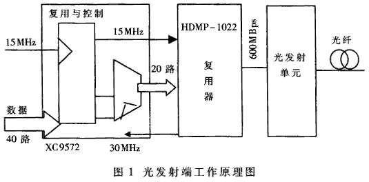
1 System principle and structure
The optical fiber transmission system of high-speed video signals mainly includes multiplexing, optical transmission, optical reception, demultiplexing, control circuits, and PCI transmission interfaces. Figure 1 is a schematic diagram of the operation of the light emitting portion of the system.
The 40 channels of 15MBps obtained from high-speed video acquisition are first multiplexed by 2:1 in XC9572 to form 20 channels of 30MBps of secondary multiplexed data for HDMP-1022, which completes channel coding and converts into 600MBps PECL strings. The row data drives the light emitting module to complete the fiber launch of the data. Figure 2 is a schematic diagram of the light receiving portion.
The demultiplexing chip HDMP-1024 extracts 20 parallel data and 30MHz clock signal from the 600MBpsPECL data received by the fiber receiving module, and then performs secondary demultiplexing by XC9572, and also PCI transmission composed of FIFO and PLX9052. The card provides timing signals, and the computer obtains real-time high-speed video acquisition data through the PCI bus, and displays and processes it.
2 hardware design
The hardware design of the system mainly includes three parts: fiber transmission unit, PCI transmission unit and control unit. 
2.1 Digital optical fiber transmission unit design
The digital optical fiber transmission unit mainly performs the multiplexing and demultiplexing functions of the serial-parallel data. In the design, the CIMT (CondiTIonal-Invert Master TransiTIon) channel coding method in data communication is used to encode the data. Figure 3 shows the format of the CIMT code.
The CIMT code has three frame forms: a data frame, a control frame, and a padding frame. The format of the data frame and control frame is shown in Figure 3(a). You can send any data and control information that needs to be transmitted. Each frame starts with C-Field (Coding Field), followed by D-Field (Data Field). ). The data bit composed of D-Field can be sixteen or twenty digits, and the system uses twenty bits of data; the control bit (C-Field) is composed of four data codes, and the receiving end can extract and lock the type of data. With status. The padding frame is generated when there is no data signal at the transmitting end and when the transmitting end and the receiving end establish a connection. At the main transient point of the three frames is the reference point at which the receiving end recovers the clock signal. In this system, Agilent's HDMP-1022 and HDMP-1024 are selected as the main chips for multiplexing and demultiplexing CIMT codes, and HFCT-5208 is used as a light-emitting and optical receiver to realize point-to-point fiber transmission design.
In the design of the optical transmitter, HDMP-1022's Double-Frame mode is used to realize 40-channel data transmission, and the parallel data capacity is expanded by two-stage multiplexing to 40 channels. The data is simultaneously multiplexed into one high-speed signal under the same clock control, and another bit-inverted signal is generated at the same time, and finally the light emitter is driven by its CIMT encoder output. FIG. 4 is a timing diagram of multiplexing transmissions in a Double-Frame manner. CLOCK (15MHz) is a single data acquisition clock, FLAG represents the parity field, CAV and DAV represent the control bits of the data frame and control frame, C0~C39 represents the input 40 signals, and D0~D19 is the DMT of the CIMT code. Data, STR-BOUT (30MHz) is the multiplier clock after the chip is phase-locked.
At the optical receiving end, the optical receiver converts the obtained optical signal into a high-speed electrical signal and transmits it to the HDMP-1024, which demultiplexes and extracts the reference clock signal STRBOUT (30 MHz), the data signals C0 to C39, and other states. Control signal and data clock RCLK (15MHz). FIG. 5 is a timing diagram of the Double-Frame optical receiving end.
image 3
2.2 PCI transmission unit design
In order to realize real-time recording of high-speed video signals, the PCI bus technology is utilized in the design. The PCI control chip adopts PLX9052, which combines with FIFO to realize the maximum data transmission rate of 120MBps digital input.
The PLX9052 is PCI2.1 compliant and supports low cost slave adapters. The internal includes a 64-byte write FIFO and a 32-byte read FIFO. By reading and writing FIFOs, high-performance burst data transmission can be realized; the local bus and the PCI bus clock are independent of each other, and the local bus clock frequency The range is 0~40MHz, and the clock frequency range of PCI is 0~33MHz. Some important configuration information of PCI bus and local bus can be provided through serial EEPROM. The PLX9052 supports bursty memory-mapped transfers and single-cycle memory or I/O map transfers, using 32-byte direct slave read FIFOs and 64-byte direct slave write FIFOs mapped to PCI memory and I/O space. The address in the middle is set by the PCI base register. Moreover, the local map register allows the PCI address space to be converted to a local address space. Figure 6 is a circuit diagram of the PLX9052 and FIFO interconnection, the FIFO uses IDT72205 of IDT Company.
2.3 Control unit design
The timing control unit of the whole design is completed by CPLD. At the optical transmitting end, it mainly provides 2:1 multiplexing of 40 signals, data latching and timing signals of system operation; at the optical receiving end, it is mainly demultiplexing, FWO and The PLX9052 provides the corresponding timing logic. This design selects XC9572 of Xilinx as the core chip of the control unit, and combines its online programming function to complete the timing debugging and design of the whole system.
Combined with Verilog language and schematic (sch) method, the whole system timing design is better realized. The following is a 40-way digital signal 8:1 multiplexed Verilog language design code. 
3 software design
The entire system software mainly includes the driver and system application design of the PCI transmission unit. The PCI driver under Windows includes not only the drivers for physical devices, but also the virtual device drivers for non-physical devices such as file systems. In the design, it is mainly designed for PCI driver under Windows2000. Because Windows 2000 prohibits user-mode programs from accessing I/O ports (Windows 95/98 allows user programs to directly access I/O ports), drivers that directly control physical devices are in kernel mode. The PCI driver of this design requires access to various hardware resources, so you should choose a driver mode that works at zero level.
The main development tool used to develop device drivers is the Windriver package provided by JUNGO. This package provides documentation for developing PLX9052 related devices, header files and library files needed for compilation, debugging tools, and program examples. Use the internal underlying services that can be invoked, such as DMA services, interrupt services, memory management services, installable file system services, etc., in conjunction with VC++ to complete the entire PCI device driver. This design includes the following aspects:
(1) PCI device initialization 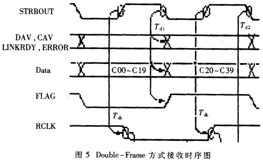
The PCI device driver first implements the identification of the PLX9052 device, the resources that address the PLX9052 device, and the service to the PLX9052 device interrupt. Mainly call the following function in the Windirver package:
WD_Open(hWD);
PCI_Get_WD_handle(&hWD);
PLX_LocateAndOpenBoard(0x10b5, 0x9052, UseInt);
(2) PCI port address operation
The PCI bus is a 32-bit bus standard. Double-word (DWORD) operations are usually performed during I/O operations. In Windows 2000, the system does not allow user programs and user-mode drivers in priority 3 to use I directly. /O instruction. Any operation on I/O needs to be done with kernel mode drivers. The author mainly calls two functions in the Windirver package to complete. 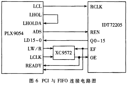
(3) Memory reading and writing
PLX9052 and the computer for data communication mainly adopt DMA mode, in the Windriver provides the corresponding memory to read two functions, through the call to it can realize the data exchange between PLX9052 and computer memory.
The application development of the entire system is based on Microsoft's VC++ development design, which can be used under the Windows 2000 operating system.
The entire optical fiber transmission system utilizes multiplexing, demultiplexing, and PCI technology to realize high-speed video digitized signal long-distance transmission and control, real-time display and other functions, the transmission distance is 15km, and the recordable data volume is 128K bytes. The design has been used in related test projects and will further improve the capacity and stability of the expanded data.
LED Driver ,Power LED Driver ,Constant Current Driver ,Constant Current LED Driver Circuit
LED Power Supply Co., Ltd. , http://www.nbleddrivers.com