1.5MHz Dual Step-Down in the MAX8529 and xDSL Modems
1 Overview
The MAX8529 is a new 1.5MHz step-down controller from Maxim Corporation. The two independent regulators in the chip operate at 180°C out-of-phase, reducing input filtering requirements and reducing EMI. The efficiency is improved, and the loss of components is also effectively reduced, which saves space on the board. In addition, the chip has the advantages of low loss and small size, and the output noise in the DSL band is very low. The MAX8529 is primarily used in xDSL modems, broadband routers, DSPs, ASICs, and FPGA power supplies.
The MAX8529 utilizes the low-side resistor of the MOSFET as a current-sensing device, eliminating the need for current-sense resistors, which protects the DC-DC structure from damage during output overload or output short-circuit. During the short circuit, the power loss can be reduced by adjusting the feedback current threshold. Because the MAX8529 includes a power-on reset output, the system can issue a reset signal when both outputs reach the regulation threshold. The main features of the MAX8529 are as follows:
â— When operating in the DSL band, the output noise is very low;
â— It can work as an input/output capacitor using a ceramic capacitor;
â— Ability to perform buck operation or boost/buck operation simultaneously;
◠has four outputs and a 90°C phase output (with two MAX8529);
â— With feedback current limit function;
â—The input voltage is 4.75V~23V;
â—The output voltage is 0V~18V (up to 6A);
â— Efficiency is greater than 90%;
â— PWM operation with fixed frequency;
â— has an adjustable switching frequency of 600kHz ~ 1.5MHz;
â— has an external SYNC input;
â— Clock output with main/secondary circuit synchronization;
â— With soft start and soft stop function;
â— The minimum delay of the RST output is 140ms;
â—With lossless current limit (no induction resistance) function;
â—Using 24-QSOP package;
◠Operating temperature is -40 to +85 °C (MAX8529EEG).
figure 1
2 MAX8529 internal functions and pin description
2.1 Internal structure of the MAX8529
The internal block diagram of the MAX8529 is shown in Figure 1. It consists of a PWM comparator, a ramp regulator, an oscillator, a 5V linear regulator, a soft-start DAC, and undervoltage lockout. The controller can derive two outputs from the 4.75V to 23V input, and each output can be adjusted from 1V to 18V. Input voltage ripple and total RMS input current ripple are reduced with a synchronous 180°C out-of-phase output operation. An external resistor can be used to adjust the switching frequency (600k to 1.5MHz). To implement an alternative, the controller can be synchronized to an external clock generated by another MAX8529 or to a system clock. A MAX8529 can produce an in-phase or 90°C phase difference output. Since the synchronous clock signal can generally be provided by another controller, the two controllers can operate in two phases or four phases (each phase shifts 90°C). )operating. In addition, the unit also features soft start and soft stop.
The MAX8529 buck converter provides a PWM voltage mode control for each phase output (Figure 1). Since it can be divided by either the internal oscillator or the external clock to drive the SYNC input, the clock signal is generated. The switching frequency of each controller is equal to half of the oscillation frequency (fSW = fOSC/2). In addition, the internal transconductance error amplifier produces a complete error voltage at the COMP side and a high precision DC output. The duty cycle can be determined at the COMP terminal using a PWM comparator and a ramp generator. On the rising edge of each clock, the high-side MOSFET of REG1 is turned on and remains in this state until the appropriate duty cycle or maximum duty cycle is reached. The second high-side MOSFET (REG2) is turned on at the falling edge of the clock. During each high side MOSFET turn-on, the corresponding induced current ramps up. 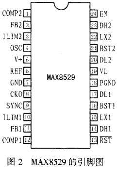
During the second half of the switching cycle, the high-side MOSFET is turned off, the low-side MOSFET is turned on, the induced current ramps down, energy is released, and the output current is supplied. In the event of an overload, when the induced current exceeds the selected valley current threshold, the high-side MOSFET remains non-conducting on the corresponding clock edge, while the low-side MOSFET remains on to allow the induced current to continue to drop.
2.2 MAX8529 Pin Description
The pinout of the MAX8529 is shown in Figure 2. The function of each pin is as follows:
1,12 feet (COMP2, COMP1): compensation terminals of regulators 2, 1, respectively;
2, 11 feet (FB2, FB1): feedback input terminals of regulators 2 and 1, respectively, which are connected to a resistor divider between REG2 and REG1 to GND, which can be used to adjust the output voltage ( 1V ~ 18V).
3, 10 feet (ILIM2, ILIM1): are the current limiting adjustment terminals of regulators 2 and 1, respectively. If ILIM2, ILIM1 to VL are connected respectively, the current-limit threshold of PGND-LX2 and PGND-LX1 defaults to 100mA. By connecting a resistor RILIM2 and RILIM1 between ILIM2 and ILIM1 to GND, the current-limit thresholds VITH2 and VITH1 of REG2 and REG1 can be adjusted to 50mV (RILIM2=100kΩ) to 300mV (RILIM2=600kΩ).
4 feet (OSC): Oscillation input. Since the controller generates a clock signal by dividing the oscillator, the switching frequency is equal to half of the synchronous frequency (fSW = fOSC/2). Connect a resistor ROSC between OSC and GND to generate a switching frequency of 600kHz?ROSC=10kΩ?~1500kHz?ROSC=4kΩ?. When connecting an external clock to SYNC, the controller still requires ROSC, and ROSC should be selected to meet half of the SYNC input.
5 feet (V+): Input power supply voltage (4.75V ~ 23V).
6-pin (REF): 2V reference output. Use it with a 0.22μF or larger ceramic capacitor connected to GND.
7 feet (GND): analog ground.
Pin 8 (CKO): Clock output for external 2-phase or 4-phase synchronous clock output.
9-pin (SYNC): Synchronous or optional clock input. SYNC has three modes of operation, connecting SYNC to a 1200kHz to 2800kHz clock for external synchronization; connecting SYNC to GND can be used as a master controller for 2-phase operation; connecting SYNC to VL can be used as a master controller for 4-phase operation. .
image 3
Pin 13 (RST): Power-on reset terminal. When the two output voltages are above 10% of the regulation point, RST is low. When the system completes the soft start, the two output voltages exceed 90% of the normal output voltage (VFB -> 0.9V), then the system will turn RST into a high-impedance state after a 140ms delay, and keep the two outputs Maintain a high resistance state when stable. A logic level can be generated by connecting a resistor between the RST and the logic input.
14, 23 feet (DH1, DH2): respectively, the high side gate driver output of regulator 1/2, DH1 generally varies between LX1 and BST1, and DH2 typically varies between LX2 and BST2.
15, 22 feet (LX1, LX2): respectively, the connection of the regulator 1/2 external sensor, LX1/LX2 can be connected to the switch end of the sensor, so that LX1, LX2 as a lower input source Drive DH1, DH2 high side gate drivers.
16, 21 feet (BST1, BST2): respectively, the booster fast capacitor connection of regulator 1/2, designed to connect an external ceramic capacitor to the BST1 to LX1 and BST2 to LX2 terminals respectively.
17, 20 feet (DL1, DL2): respectively, the regulator 1/2 low side gate driver output, the output voltage of DL1, DL2 generally varies between PGND and VL.
18 pin (PGND): power ground.
19-pin (VL): Internal 5V linear regulator output.
Pin 24 (EN): High level enable. When the terminal is logic low, the two controllers in the circuit will be turned off. When the end is connected to VL, the operation will remain.
Figure 4
3 MAX8529 application circuit
The application circuit of the MAX8529 is shown in Figure 3. All of the features of the MAX8529 come from low-fading 5V regulators. The regulator's maximum input voltage (V+) is 23V, and a 4.7μF ceramic capacitor should be connected between the output (VL) and PGND. Since the VL fading voltage is nominally 500 mV, VL is 5 V when the V+ value is greater than 5.5V. When the VL is below 4.5V, the undervoltage lockout circuit will lock the two regulators. The VL linear regulator can output more than 50mA to the IC to excite the low side gate driver to charge the external boost capacitor and supply a small external load.
The gate drive voltage of the high side switch is provided by a fast capacitor boost circuit (see the circuit shown in Figure 3). After startup, the capacitor will charge to 5V. During the second half cycle, the low-side MOSFET turns off and turns off an internal switch of BST- and DH-, while turning on the high-side MOSFET.
SYNC has two functions: one is to synchronize the clock output (CKO) selected from the controller; the other is to synchronize the clock input with the MAX8529's external clock signal. Therefore, the MAX8529 has both master and slave functions. The role of the CKO is to provide a synchronized clock signal as the switching frequency of the MAX8529. It can be in phase with the controller's sync signal (SYNC = GND) or 90 ° C phase (SYNC = VL). The three control modes that the MAX8529 can provide are as follows:
First, when SYNC is connected to GND, the output frequency of CKO is equal to the switching frequency of REG1 (fCKO=fDH1), and the two signals are in phase. At this time, if the signal is synchronized with the slave controller, 2-phase operation can be provided.
Second, when SYNC is connected to VL, the output frequency of CKO is equal to twice the switching frequency of REG1 (fCKO=2fDH1). At this time, the two signals are 90° out of phase, so that the system signal can be provided when synchronizing with the controller. 4-phase operation.
Third, when SYNC is driven by the external oscillator, it can be seen that the SYNC input signal is divided by 2 to generate the controller clock (fSW=fSYNC/2). At this time, the period change of REG1 will be performed on the rising edge of the internal clock signal. fCKO=fDH1, and in phase. However, ROSC is still needed at this time, and the internal oscillation frequency is half of the synchronous frequency (fOSC=fSYNC/2).
4 Conclusion
Because the two independent regulators inside the MAX8529 use a synchronous 180°C out-of-phase operation output, the input filtering requirements are reduced, EMI is reduced, and efficiency is greatly improved compared to conventional non-inverting outputs. It also reduces component losses and saves board space. Especially in the DSL frequency band, its output noise is very low, so it has been widely used in xDSL modems, broadband routers, DSP, ASIC and FPGA power supplies.
Lightweight Suitcases ,Hand Luggage Suitcase ,Best Lightweight Luggage ,Lightweight Hard Suitcase
Hair Weaving & Hair Weft Co., Ltd. , http://www.nboutdoors.com