Application of HAC technology in GSM mobile phones
HAC is the abbreviation of Bearing Aid Compliance, which is used to measure the compatibility of mobile phones and hearing aids working together. This indicator is to ensure that people with hearing impairment can use the same mobile phone as ordinary people.
This article refers to the address: http://
Wireless telephones represented by GSM have been widely used in recent years. However, the requirements of HAC have gradually emerged in recent years. Mandatory requirements already exist in some countries, such as the United States. China also has its own HAC standard, but it is not mandatory. Compared to the design of antennas and RF circuits, HAC is much more difficult to design. This article will combine some mass-produced products as an example to illustrate how to effectively reduce the near-field radiation of electric and magnetic fields in specific areas when designing GSM mobile phones to achieve the ability to work with hearing aids. The design ideas and methods presented here can also be applied to other wireless terminals.
Basic architecture introduction
Figure 1 is a simplified schematic diagram of the structure of the mobile phone. The position of the antenna is at the lower end of the mobile phone, and the handset of the mobile phone is placed at both ends of the mobile phone. Therefore, as shown in Figure 1, the electric and magnetic fields in the test area need to fall below the HAC requirements. This article discusses a technique that reduces the electric and magnetic field radiation in the test area without reducing the radiation efficiency of the antenna.
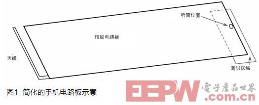
Figure 2 is a schematic diagram of this technique. In FIG. 2, the length of the metal piece must be smaller than the length of the printed circuit board 1. That is to say, there must be sufficient space from the edge of the printed circuit board 1 to the test area. This is the key point of this technology. In Fig. 2, two printed wiring boards, including the upper metal parts, are connected at least at the connection point 1 and the connection point 2. This connection ensures that the resonance point of the antenna does not change.
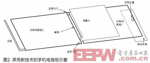
In practice, the metal piece in Figure 2 may vary depending on the actual situation. But its basic working principle is not changed, as explained below.
theoretical analysis
The working principle of this technique will be described below with reference to Figs. 1, 2, 3 and 4. Figure 3 is a current distribution diagram of a bar phone, and Figure 4 is a current distribution diagram after adding the technology to a bar phone.
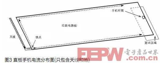

In general, the current distribution on the phone is gradually diminished from the antenna feed to the other end of the board (see Figure 3). In Figure 3, the magnitude of the current is varied and the direction of the current is also varied. The current intensity is reduced to zero at the end of the board. The reduction in current intensity to zero means the accumulation of charge, so the induced electric field plays a dominant role here. At the same time, this varying electric field produces a corresponding magnetic field. This produces corresponding electric and magnetic field changes in the test area. The static magnetic field and the electrostatic field do not cause any current to be generated by the metal devices inside the field. Therefore, it is sufficient to mainly consider the changing electromagnetic field in the test area. Based on the above analysis, if we can remove the changing electromagnetic field from the test area, we have achieved the design goal.
In Figure 2, the printed circuit board is divided into two sections by a slot. These two parts are only connected at connection point 1. At the same time, a metal plate is added in parallel directly above the printed circuit board 1. This metal plate and circuit board 2 are connected together at a connection point 2. This makes it possible to forcibly divide the current flowing between the printed circuit boards 1 and 2 into two parts. Some of them flow as they are. The other part becomes a flow between the metal plate and the printed circuit board 2. Thus, the total amount of current on the printed circuit board 1 is lowered. If we can not keep the edge of the metal plate and the printed circuit board 1 at a certain distance, then the two corresponding electromagnetic fields cannot be linearly superimposed, so as to effectively reduce the electromagnetic field in the test area.
The basic idea of ​​this technique is to remove a portion of the end-induced charge from its original location. Since the electromagnetic field is three-dimensionally radiated, the speed of the electromagnetic field decreases much faster than the moving distance. The movement of the accumulated charge over a small spatial distance can cause a very large change in the electromagnetic field strength in the test area.
After the metal plate is added, since the printed circuit board 1 and the metal plate have a strong coupling, the two printed circuit boards together with the metal plate serve as the ground of the antenna. The size of the ground has not changed. Therefore, the resonance and radiation of the antenna will not change, thus effectively achieving the purpose of keeping the performance of the antenna unchanged while effectively reducing the electromagnetic field of the test area.
Computer simulation and test results
In this section, we mainly introduce how to use computer simulation and sample testing to further verify our design ideas. The model used in computer simulation is the same as in Figures 1 and 2.
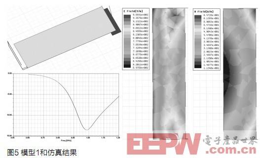
First of all, we have built the same model in the computer as in Figure 1. The size of the whole model is set to 100mm × 40mm. This size is the actual size of a typical mobile phone. All the characteristics of metal materials use the characteristics of copper. The resonance point is set at 1 GHz, and the simulation model and simulation results are shown in Fig. 5.
Model 2 is built based on Model 1. We used a 38mm × 2mm gap to divide the printed circuit board into two, and added a 40mm × 40mm metal plate (Figure 2), the distance between the metal plate and the printed circuit board is 4mm. The model and simulation results are shown in Figure 6.
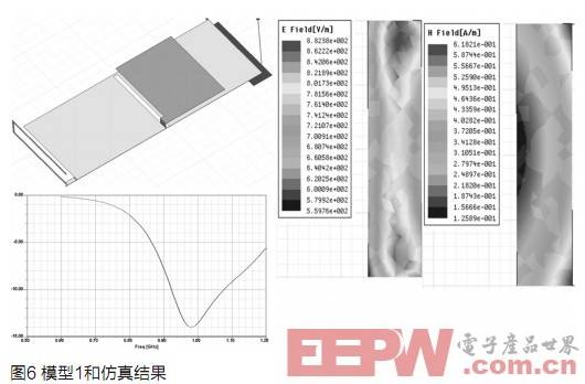
The graphs in Figures 5 and 6 are the intensity of the electromagnetic field in the test area. Comparing Fig. 5 with Fig. 6, it can be clearly seen that the value of the electromagnetic field in Fig. 6 is relatively low. (Please refer to Table 1)


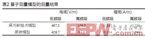
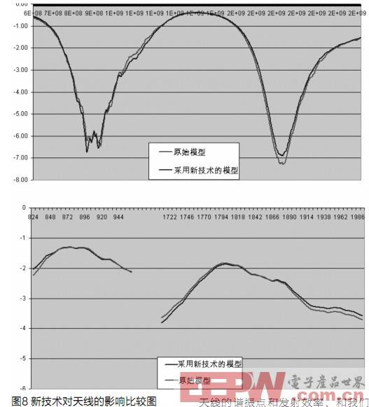
To further validate the effectiveness of this technique, we produced a realistic model for verification to validate our design ideas. Figure 7 is a picture of the verification model with the addition of new technology. Table 2 shows the results of the electromagnetic field test. Figure 8 is a comparison of the antenna resonance point and emission efficiency. The above is a comparison of the resonance points, and the lower part is a comparison of the emission efficiencies. As can be seen from the test results, this technique is the same as we imagined. Comparing computer simulations and tests, the differences are: 1) Computer simulation uses one frequency, and two frequencies are used in the test; 2) The test frequency and simulation frequency are not completely consistent. However, it can be seen from the test results that this scheme works, and can simultaneously reduce the value of the electromagnetic field in the test area of ​​different frequency bands, and does not affect the resonance point and emission efficiency of the antenna, which is completely consistent with our assumption.
In the actual design work, the shape and size of the metal sheet can be fine-tuned to achieve the best results.
From the simulation and measured data, we can conclude that this technology is effective and the above theoretical analysis is credible and can be used to guide the design work.
2760 applications in Nokia
Like the development of other technologies, new technologies are created to meet the needs of practical work. The purpose of developing this technology is to solve problems in the middle of actual work.

The N2760 is a folding machine, as shown in Figures 9 and 10. The antenna and HAC test area are at the two ends of the handset, and the two printed circuit boards are connected by a flexible printed circuit board.

The red part in Figure 10 is a metal plate that is used to reduce the electromagnetic field in the test area. It is connected to the printed circuit board 2 by the connection chain of the folding machine, and its shape is optimized according to the specific mobile phone design environment. Table 3 is the measured results.
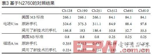
Figure 11 is a comparison of the radiation efficiencies of the antennas in different frequency bands before and after implementation of the present technology. It can be seen from the figure that there is no significant change in the resonance point and efficiency of the antenna before and after the use of the new technology. However, in the terrestrial frequency band, the bandwidth of the antenna is reduced after using the new technology. The change in bandwidth is due to the frequency selectivity of the metal piece. No more detailed discussion here.

Conclusion
Based on theoretical analysis, computer simulations, model measurements, and actual product measurements, we can consider this technique to be effective. And we successfully applied this technology on the Nokia N2760. The phone also passed the FCC HAC M3 standard certification and the US carrier TMO requirements for antenna radiated power and sensitivity.
Vending Machine,Electric Beverage Dispenser,Sapoe Juice Dispensing Machines
Instant Coffee Machine Co., Ltd. , http://www.nscoffeemachine.com