High-speed ADC PCB layout and routing skills
In high-speed analog signal chain designs, printed circuit board (PCB) layout requires consideration of many options, some of which are more important than others, and some depend on the application. The final answer is different, but in all cases, the design engineer should try to eliminate the error of best practices without over-considering every detail of the place and route. This article, which is recommended for you today, will start with the exposed pad and talk about decoupling and layer capacitance, layer coupling, and grounding.
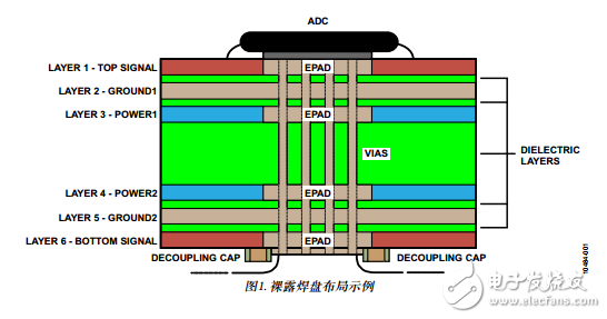
The exposed pad (EPAD) is sometimes overlooked, but it is important to get the most out of the signal chain and the device to dissipate heat.
The exposed pad, which ADI calls pin 0, is the pad under most devices today. It is an important connection through which all internal grounding of the chip is connected to the center point below the device. I wonder if you noticed that there are currently no ground pins in many converters and amplifiers because of the exposed pad.
The key is to properly pin (ie solder) this pin to the PCB for a secure electrical and thermal connection. If this connection is not secure, confusion can occur, in other words, the design may not work.
Achieve the best connectionThere are three steps to achieving optimal electrical and thermal connections with exposed pads
First, where possible, the exposed pad should be replicated on each PCB layer in order to form a dense thermal connection with all ground and ground planes for fast heat dissipation. This step is related to high power devices and applications with high channel counts. On the electrical side, this will provide a good equipotential bonding for all ground planes.
The exposed pad can even be replicated on the underlying layer, which can be used as a place to decouple the thermal ground plane and mount the bottom side heat sink.
Second, the exposed pad is divided into multiple identical parts, like a checkerboard. Use a wire mesh cross grill on the open exposed pad or use a solder mask. This step ensures a robust connection between the device and the PCB. During the reflow assembly process, it is not possible to determine how the solder paste flows and ultimately connects the device to the PCB. Connections may exist but are unevenly distributed. Maybe only get one connection, and the connection is small, or worse, at the corner. Dividing the exposed pad into smaller sections ensures that each zone has a connection point for a more secure, evenly connected exposed pad.
Third, it should be ensured that all parts have vias connected to the ground. Each area is usually large enough to hold multiple vias. It is important to fill each via with solder paste or epoxy before assembly. This step is important to ensure that the exposed pad solder paste does not flow back into these via holes and affect proper connections.
Decoupling and layer capacitanceSometimes engineers ignore the use of decoupling by simply dispersing many capacitors of different sizes on the board to connect the lower impedance power supply to ground. But the problem remains: How much capacitance do you need? Many related literatures have shown that many capacitors of different sizes must be used to reduce the impedance of the power transfer system (PDS), but this is not entirely true. Instead, simply select the correct size and the correct type of capacitor to reduce the PDS impedance.
Layer couplingSome layouts inevitably have overlapping circuit layers. In some cases, it may be a sensitive analog layer (such as power, ground, or signal), and the lower layer is a high-noise digital layer.
This is often overlooked because the high noise floor is on the other layer - below the sensitive analog layer. However, a simple experiment can prove that this is not the case. Taking a certain layer as an example, a signal is injected at any layer. Next another layer is connected and the adjacent layer is cross-coupled to the spectrum analyzer.
Separate groundThe most common question asked by analog signal chain designers is: Should the ground plane be divided into AGND and DGND ground planes when using the ADC? The simple answer is: depending on the situation. The detailed answer is: usually not separated. Why not? Because in most cases, blindly separating the ground plane will only increase the inductance of the return path, which brings more harm than good.
Networking Keystone Jacks, Punch Down Type Terminals.China Network & Accessories,Networking KEYSTONE Jacks supplier & manufacturer, offer low price, high quality Punch Down Type Terminals,, etc.
Networking KEYSTONE Jacks, Punch Down Type Terminals.China Network & Accessories,Networking KEYSTONE Jacks supplier & manufacturer, offer low price, high quality Punch Down Type Terminals,, etc.
Networking KEYSTONE Jacks, Punch Down Type Terminals.China Network & Accessories,Networking KEYSTONE Jacks supplier & manufacturer, offer low price, high quality Punch Down Type Terminals,, etc.
Network & Accessories,Networking KEYSTONE Jacks, Punch Down Type Terminals
ShenZhen Antenk Electronics Co,Ltd , https://www.antenk.com