Design of intelligent carrier module based on low-voltage power line
Low-voltage power line carrier communication (Power Line CommunicaTIon) refers to a technology that uses the existing low-voltage power line network as a transmission medium to realize data transmission and information exchange [1]. The characteristics of low-voltage power line carrier communication, such as wide distribution, no need to build, plug and play, and convenient movement, are very attractive to meet people's needs. The technology is now increasingly attracting people's attention.
In China, even the mature low-voltage power line communication products of European and American countries are not ideal for use in our country, and even cannot be used. Therefore, the design purpose of the low-voltage power line smart carrier module is to develop a cost-effective carrier communication module, select the appropriate modulation and demodulation technology, and carry out accurate, stable and long-distance data transmission.
2.1 Overall design plan The main function of the low-voltage power line smart carrier module is: the external control system transmits the data to be transmitted to the P89LPC932 through the standard UART, I2C or SPI serial interface, and then the data is modulated to the microcontroller and the modulation circuit. At the same time, the data modulated on the low-voltage power line is demodulated by the demodulation circuit part and the data on the low-voltage power line is transmitted to the external control system through the P89LPC932 standard UART, I2C or SPI serial interface for corresponding deal with. The overall block diagram of its module is shown in Figure 1 [2]. The design uses an 8-bit single-chip microcomputer P89LPC932 produced by PHILIPS as the controller, and uses a cost-effective analog and digital electronic device and some capacitors and resistors to form a phase detection circuit and a modulation and demodulation circuit.

2.2 Principle of phase pulse modulation and demodulation method Principle of phase pulse modulation and demodulation method [3-4] is to add an instantaneous zero pulse signal at a fixed phase of each cycle of the sinusoidal low-voltage power line. When the signal is modulated in a cycle of sinusoidal alternating current, an instantaneous zero pulse is generated at a fixed phase point. When there is no modulation signal in a cycle of sinusoidal alternating current, no instantaneous zero pulse appears. Therefore, the presence or absence of instantaneous zero pulse is used to identify the "1" and "0" signals carried on the low-voltage power line.
2.3 Hardware design of the system
2.3.1 Selection of microcontroller In this design, an 8-bit microcontroller P89LPC932 microcontroller produced by PHILIPS was selected [5]. P89LPC932 is a single-chip package microcontroller, suitable for many requirements of high integration, Low cost occasions. Its main features are: at the same clock frequency, its speed is 6 times that of the standard 80C51 device, only a lower clock frequency is needed to achieve the same performance, reducing power consumption and EMI; enhanced UART, 400kHz byte Mode I2C communication port, SPI communication port; configurable on-chip oscillator and its frequency range and RC oscillator options; programmable I / O port output mode: quasi-bidirectional port, open-drain output, push-pull and input only Features.
2.3.2 Design of the phase detection circuit The phase detection circuit designed by this system is to fix the phase point of the sinusoidal alternating current, so that the phase detection circuit generates a square wave signal with a certain duty cycle, and the square wave provides 50Hz to P89LPC932 The external interrupt signal, the hardware schematic of the phase detection circuit is shown in Figure 2:
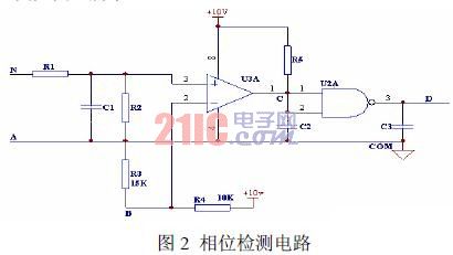
In the figure, point N is connected to the neutral line of 220V AC, point A is connected to the live line of 220V AC, and it is also used as the analog ground COM terminal of the system. R3 and R4 form a path through the series connection method. From the voltage division formula, the voltage at point B is 6V. That is, the inverting input of the voltage comparator U3A is clamped at 6V, and the N point and A point form a loop through the resistors R1, R2 and capacitor C1. From the circuit principle, it can be seen that the The power frequency alternating current has the same frequency but the amplitude of the sinusoidal alternating current is reduced. When the voltage of the input terminal of the voltage comparator U3A is higher than the voltage of the reverse input terminal by 6V, the output terminal of the voltage comparator U3A outputs a high-level signal of 10V. When the voltage of the non-inverting input terminal of the voltage comparator U3A is lower than the voltage of the inverting input terminal by 6V, the output terminal of the voltage comparator U3A outputs a low-level signal of 0V. Therefore, a square wave signal with a certain duty ratio is obtained as an external interrupt input signal of P89LPC932. It can be seen from the calculation that the high-level duration of the square wave signal is 12ms, and the low-level duration is 8ms.
2.3.2 Design of the signal modulation circuit The function of the signal modulation circuit is mainly to complete the modulation of the data sent by the microcontroller on the low-voltage power line after the P89LPC932 receives the external interrupt input signal, so as to realize the transmission of the data on the power line. The hardware schematic diagram of the signal modulation circuit is shown in Figure 3.
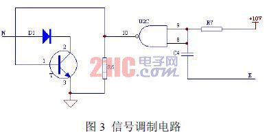
In the figure, point E is the data input terminal for signal modulation by P89LPC932. When transmitting a bit of data "0", point E is always a high-level signal with an amplitude of 10V. At this time, the two inputs of the voltage comparator U2C The terminal is in a high state and the output is in a low state. There is no voltage difference between the base and the emitter of the high power transistor T, and T is not conductive, so there is no zero pulse signal modulated onto the low voltage power line; When the bit data is "1", a low-level signal with a short duration appears at point E (the pulse width of this low-level signal is determined jointly by R7, C4 and the data modulation procedure). Since the voltage across the capacitor C4 cannot be abrupt, a zero pulse signal appears at the two input terminals of the voltage comparator U2C, a pulse signal with an equal amplitude of 10V appears at the output terminal, and a voltage appears between the base and the emitter of the transistor T Poor, the transistor T is turned on, so that the live line and the zero line of the sinusoidal alternating current are turned on instantaneously, and a zero pulse signal appears on the power line.
2.3.2 Design of the signal demodulation circuit The function of the signal demodulation circuit is mainly to demodulate the modulated signal on the low-voltage power line from the power line and send it to the P89LPC932 for the microcontroller to process accordingly. The hardware schematic diagram is shown in Figure 4:
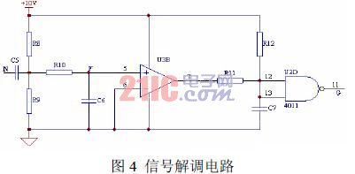
In the figure, point N is the neutral line of the low-voltage power line. Capacitor C5 plays the role of low frequency filtering. The modulated signal on the power line enters the demodulation circuit from N. Resistors R8 and R9 form a voltage divider circuit. The DC component of the voltage at point F is:
In the design, choose the appropriate resistance value, take 3.7 FV = V. Capacitor C5 and resistor R9 also form a voltage divider circuit, so that the amplitude of the sinusoidal AC voltage across R9 is less than 3.7V. Ensure that the voltage on the same input terminal of the voltage comparator U3B is always higher than the voltage on the reverse input terminal when a bit of data "0" is transmitted on the power line, and the output at point G is always zero. When a bit of data "1" is transmitted on the power line, a zero pulse signal appears at the 6V phase of the sinusoidal alternating current, so a voltage pulse with an amplitude lower than the signal ground will be instantaneously generated at the same input terminal of the voltage comparator U3B A pulse signal is generated at the output of the comparator U3B, and a pulse signal with an amplitude of 10V is generated at point G via the reverse of the NAND gate, which is input to the microcontroller through the isolation of the optocoupler.
This software uses modular, structured design. The main program is responsible for the initialization of each function register, waiting to send data and other functions. The interrupt handler is responsible for receiving external input data, sending and receiving data through the power line, and other functions.
3.1 Introduction of improved Modbus protocol An important point of software design is the formulation of communication protocol for low-voltage power line smart carrier module. In this design, the improved Modbus protocol is used. It is improved by the fusion of ASCII transmission mode and RTU transmission mode of Modbus protocol. This protocol realizes the read and write operations of the master carrier module to the slave carrier module. The frame formats are as follows:
3.1 Software design of carrier data transmission and reception Carrier data transmission and reception are implemented in the external interrupt subroutine of the microcontroller P89LPC932. The program flow chart is shown in 5:
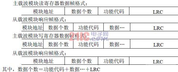
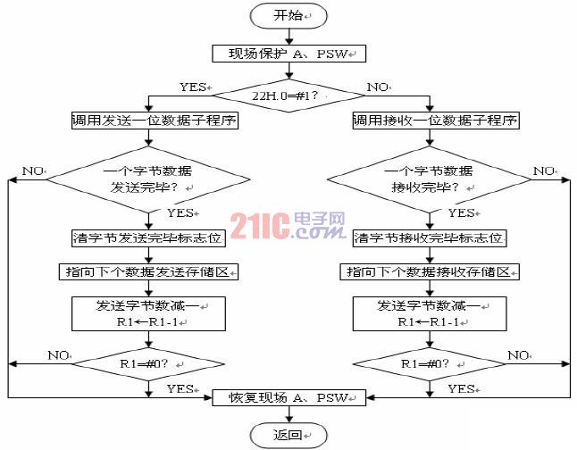
Figure 5 Carrier data transmission and reception subroutine flow chart
4 Conclusion
This article introduces a self-researched and designed intelligent carrier module based on low-voltage power line. Through the actual test of digital oscilloscope and on-site debugging in the laboratory, this design can reliably transmit data through low-voltage power line with a transmission distance of about 1000m Long transmission distance, strong anti-interference ability, can be widely used in power line meter reading, street lamp control, building automation and other occasions
Embedded Scanner,Scanner With Laser,Bar Code Scanner,2D Stationary Barcode Scanner
Guangzhou Winson Information Technology Co., Ltd. , https://www.winsonintelligent.com