Design of FSK Demodulator for 125KHz RFID Reader
Pick   To: This paper gives the FSK demodulator circuit for 125KHz non-contact RFID reader , which can demodulate FSK signal into NRZ code. This circuit is simple and practical, and can be used in various FSK modulation modes set in RFID chip. demodulation.
introduction
Many RFID chips operating at 125KHz carrier frequency , such as Microchip 's MCRF200 , MCRF250, and Atmel 's e5551 , T5557 , etc., can be set to FSK mode. If the chip is set to FSK modulation, the reader/writer (PCD) must have an FSK demodulation circuit. The FSK demodulation circuit demodulates the FSK modulated signal into an NRZ code.
This paper presents an FSK demodulation circuit, which is characterized by simple and reliable circuit and is suitable for PCD applications.
FSK modulation
The FSK modulation methods of RFID operating at 125 kHz are very similar. Figure 1 shows a waveform diagram of the FSK modulation method. As can be seen from the figure, the data rate is: carrier frequency fc/40=125K/40=3125bps . After FSK modulation, data 0 is a square wave with frequency fc/8 , ie f0=fc/8 ; 1 is a square wave with a frequency of fc/5 , that is, f1=fc/5 .
The transmitted data after FSK modulation is transmitted to the PCD by load modulation . The RF waveform is also shown in Figure 1. The modulation of the carrier is amplitude modulation.
FSK demodulation
The PCD is subjected to carrier demodulation ( usually using envelope detection ) , amplification filtering, and pulse shaping circuitry to obtain an FSK modulated signal. The FSK demodulation circuit completes the restoration of the FSK modulated signal to the NRZ code. There are many implementation methods of FSK demodulation . An FSK demodulation circuit introduced in this paper is shown in Figure 2. This circuit is simple and convenient, and can perform FSK demodulation well.
The circuit shown in Figure 2 works as follows: Trigger D1 turns the input FSK signal into a narrow pulse, that is, when Q is high, the FSK upper edge sets the Q terminal high, but since Q is low at this time , the CL terminal is low. And make the Q end back to low level. This pulse at the Q terminal zeros the decimal counter 4017 and recounts .
The 4017 counter counts the 125KHz clock . Since the data width is 40/fc=40Tc (Tc is the carrier period ) , if it is data 0 , the FSK square wave period T0=8Tc . When counting the 7th clock, the Q7 output is high, so that CLKen (CLK enable ) is high, the counter no longer counts the 8th clock, at this time Q7 is high, when the Q output of the flip-flop D1 is under When a FSK waveform is skipped, the Q terminal output of flip-flop D2 is low. The FSK waveform jumps up and resets the counter and recounts. Thus, the FSK data corresponding to the frequency of the waveform of 0, Q output of the flip-flop D2 is low, that is, data 0 of the NRZ code level.
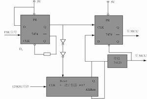
Figure 2 Â FSK demodulation circuit
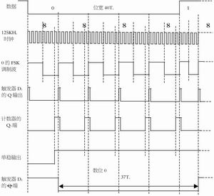
Figure 3 Â Demodulation waveform legend for digit 0 ( followed by bit 1)
When the data 1, since the FSK waveform period T1 = 5Tc, so the pin Q7 of counter 4017 is always low, during which the Q output of the flip-flop D2 is kept high, that is, NRZ data level one.
The demodulated waveform of data 0 is shown in Figure 3 . Seen from the figure, if the bit 0 is followed 0, then the bit width of 40Tc, followed if the bit is 1, the bit width which is 37Tc, short three clock cycles. Bit 1 follows the bit 1 and its bit width remains at 40Tc. If its immediate bit is 0 , its bit width is 43Tc . Therefore, the interleaving of bit values 0 and 1 does not cause the propagation of the bit width error, but is compensated. ± 3 clock errors will not affect the correctness of the MCU alignment.
The up-jump change generated by the one-shot circuit provides the trigger terminal D2 with the CL -level level of normal operation , and also informs the MCU that the output data of the flip-flop D2 is valid thereafter . The one-shot circuit can be 74HC123 , which is a repeatable triggering one-shot circuit that can automatically start and shut down the demodulator.
RFID chip FSK usually have multiple modes, such as in one of four modes e5551 (Table 1), the analysis of the circuit described above corresponds FSK1a, but FSK1, just to the output terminal Q of the flip-flop D2 Just fine. If FSK2 is used , the output of the counter can be changed to Q9 .
For different data rates, only the bit width is different and does not affect the demodulation result.
Conclusion
This circuit is simple and reliable and has been used in water meter readers.
Peel Mask PCB
Peel able masks are used in order to protect selected solder holes against plugging during mass soldering or to protect carbon elements and gold plated contacts during mass soldering. Peel able masks are screen printed.
Requirements
• The peelable mask must adhere sufficiently well to the PCB so that it does not peel off when handled correctly.
• It must be able to endure a two to three time soldering process without peeling off, but must remain detachable.
•After soldering of the PCB, the peelable mask must be able to be detached – preferably in one piece. In case of metallized holes, no mask
residue must be left in the drill holes or on the surface of the PCB. In the case of non-metallized drill holes, however a certain amount of residue
can remain.
• The peelable mask must be able to resist conventional solvents such as chlorinated and fluorinated hydrocarbons, isopropanol, conventional
fluxes and similar.
• Particular requirements: The roughness U of the edge of the mask can be 0,5 mm from the tip to the base (left figure
below).
Peel Mask Board,Green Peel Mask Board,Quick Turn Peel Mask Board,Mask Board
Storm Circuit Technology Ltd , http://www.stormpcb.com