How is the dma controller register configured?
The DMA (Direct Memory Access) controller is a unique peripheral that transfers data inside the system and can be thought of as a way to connect internal and external memory to each DMA-capable peripheral through a dedicated bus. Controller. It belongs to the peripheral because it is transmitted under the program control of the processor.
In general, the DMA controller will include an address bus, a data bus, and control registers. A highly efficient DMA controller will have the ability to access any resource it needs without the intervention of the processor itself, it must be able to generate an interrupt. Finally, it must be able to calculate the address inside the controller. [2]
A processor can contain multiple DMA controllers. Each controller has multiple DMA channels and multiple buses that are directly connected to memory banks and peripherals, as shown in Figure 1. Two types of DMA controllers are integrated in many high performance processors. The first type, commonly referred to as the "system DMA controller", enables access to any resource (peripherals and memory). For this type of controller, the number of signal cycles is counted by the system clock (SCLK). Take ADI's Blackfin processor as an example, the frequency can be up to 133MHz. The second type, called the Internal Memory DMA Controller (IMDMA), is dedicated to inter-access operations between locations where internal memory is located. Since access occurs internally (L1-L1, L1-L2, or L2-L2), the count of the number of cycles is based on the core clock (CCLK), which can exceed 600 MHz.
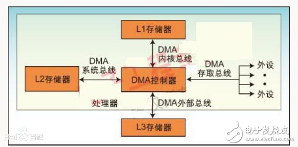
Figure 1: System and memory DMA architecture.
Each DMA controller has a set of FIFOs that act as a buffer between the DMA subsystem and the peripheral or memory. For MemDMA (Memory DMA), both the source and destination of the transmission have a set of FIFOs. When the resources are tight and the data transfer cannot be completed, the FIFO can provide a temporary storage area for the data, thereby improving performance.
Because you usually configure the DMA controller during code initialization, the kernel only needs to respond to the interrupt after the data transfer is complete. You can program the DMA control to move data in parallel with the kernel while allowing the kernel to perform its basic processing tasks—those that should let it focus on completion.
How to configure the DMA registerThis article does not say anything, is the status code.
1. There are three cases of special codes "00" and "FF" and other start codes:
1 has appeared after a series of other codes: "00" or "FF", then the motherboard is OK.
2 If there is no error in the CMOS setting, the non-critical fault will not affect the continuation of the BIOS self-test, and eventually "00" or "FF" will appear.
3 When the power is turned on, "00" or "FF" or other start code appears and the board does not run.
2, this table is sorted according to the code value from small to large, the order of the card in the code is uncertain.
3. Undefined code tables are not listed.
4, for different BIOS (commonly used AMI, Award, Phoenix) with the same code represents a different meaning, so you should find out which type of BIOS your computer belongs to, you can check your computer use The manual, or directly from the BIOS chip on the motherboard, can also be seen directly when the screen is launched.
5, there are a few motherboard PCI slots only the first part of the code appears, but the ISA slot has a complete self-test code output. At present, it has been found that there are very few original machine motherboards with no code output in the ISA slot, and the PCI slot has full code output. Therefore, it is recommended that you change the dual slot card to another slot when the viewing code is unsuccessful. . In addition, the different PCI slots of the same motherboard, some slots have a complete "code sent out, such as the DELL810 motherboard only a PCI slot near the CPU has a complete code display, has been changed to "00" or "FF", while other slots go Until "38", it will not continue to change.
6, the time required to reset the signal ISA and PCI are not necessarily synchronized, so it is possible that the ISA starts to code, but the PCI reset light is not extinguished, so the PCI code stops at the start code.
Code Award BIOS Ami BIOS Phoenix BIOS or Tandy 3000 BIOS
00. The configuration of the system has been displayed; the INI19 boot load will be controlled. .
01 Processor Test 1, Processor Status Verification, if the test fails, the loop is infinite. The test of the processor registers is about to begin, and the non-maskable interrupts are about to be deactivated. CPU register test is in progress or failed.
02 Determine the type of diagnosis (normal or manufactured). If the keyboard buffer contains data, it will fail. Disable non-maskable interrupts; start with a delay. CMOS write/read is in progress or fails.
03 Clear the 8042 keyboard controller and issue the TESTKBRD command (AAH). The power-on delay has been completed. The ROM BIOS checks that the component is in progress or is malfunctioning.
04 Reset the 8042 keyboard controller and verify TESTKBRD. Keyboard controller soft reset / power-on test. The test of the programmable interval timer is in progress or fails.
05 If the manufacturing tests 1 to 5 are repeated repeatedly, the 8042 control status can be obtained. Soft reset/power on has been determined; ROM will be started soon. The DMA is ready to go on or fail.
06 Make the chip initial preparation, disable video, parity, DMA chips, and clear DMA chips, all page registers and CMOS shutdown bytes. The ROM has been started to calculate the ROM BIOS checksum and to check if the keyboard buffer is cleared. The DMA initial page register read/write test is in progress or fails.
07 Processor Test 2, verify the operation of the CPU registers. The ROM BIOS checks that the sum is normal, the keyboard buffer is cleared, and a BAT (Basic Guarantee Test) command is issued to the keyboard. .
08 Make the CMOS timer initial preparation, and normally update the timer loop. A BAT command has been issued to the keyboard, which will write the BAT command. The RAM update check is in progress or fails.
09 EPROM checks the sum and must be equal to zero before passing. Verify the basic guarantee test of the keyboard, then verify the keyboard command byte. The first 64K RAM test is in progress.
0A Makes the video interface initial preparation. The keyboard command byte code is issued, and the command byte data is about to be written. The first 64K RAM chip or data line failed and shifted.
0B Test 8254 channel 0. Write the keyboard controller command byte, which will issue the lock/unlock commands for pins 23 and 24. The first 64K RAM odd/even logic failed.
0C Test 8254 channel 1. The keyboard controller pins 23, 24 have been blocked/unlocked; a NOP command has been issued. The address line of the first 64K RAN is faulty.
0D 1. Check if the CPU speed matches the system clock. 2. Check if the programmed value of the control chip meets the initial setting. 3, video channel test, if it fails, honk. The NOP command has been processed; then the CMOS shutdown register is tested. Parity failure of the first 64K RAM
0E Test CMOS shutdown byte. CMOS off register read/write test; the CMOS checksum will be calculated. Initialize the input/output port address.
0F tests extended CMOS. The CMOS checksum has been calculated to write the diagnostic byte; CMOS begins initial preparation. .
10 Test DMA channel 0. CMOS has been initially prepared, and the CMOS status register is ready for the date and time. The 0th bit of the first 64K RAM is faulty.
11 Test DMA channel 1. The CMOS status register has been initially prepared to disable the DMA and interrupt controllers. The first bit of the first 64DK RAM is faulty.
12 Test the DMA page register. The DMA controller 1 and the interrupt controllers 1 and 2 are deactivated; the video display is ready and port B is initially prepared. The second bit of the first 64DK RAM is faulty.
13 Test the 8741 keyboard controller interface. The video display has been deactivated and port B has been initially prepared; chip initialization/memory auto-detection will begin. The third bit of the first 64DK RAM is faulty.
14 Test the memory update trigger circuit. The chip initialization/memory automatic detection ends; the 8254 timer test is about to begin. The 4th bit of the first 64DK RAM failed.
15 Test the system memory starting with 64K. The second channel timer is half tested; the 8254 second channel timer is about to complete the test. The 5th bit of the first 64DK RAM is faulty.
16 Create an interrupt vector table for the 8259. The second channel timer test ends; the 8254 first channel timer is about to complete the test. The sixth bit of the first 64DK RAM is faulty.
17 Adjust video input/output work, if enabled with video BIOS. The 1st channel timer test ends; the 8254 0th channel timer is about to complete the test. The 7th bit of the first 64DK RAM is faulty.
18 Test video memory, if the optional video BIOS is installed, it can be bypassed. The 0th channel timer test ends; the memory will be updated soon. The 8th bit of the first 64DK RAM is faulty.
19 Test the interrupt controller (8259) mask bit of channel 1. The memory has been updated and the update of the memory will be completed. The 9th bit of the first 64DK RAM is faulty.
1A Test the interrupt controller (8259) mask bit of channel 2. The memory update line is being triggered and the 15 microsecond on/off time is about to be checked. The 10th bit of the first 64DK RAM failed.
1B Test CMOS battery level. The memory update time is 30 microseconds tested; the basic 64K memory test is about to begin. The 11th bit of the first 64DK RAM failed.
1C Tests the sum of CMOS checks. . The 12th bit of the first 64DK RAM is faulty.
1D sets the CMOS configuration. . The 13th bit of the first 64DK RAM failed.
1E measures the size of the system memory and compares it to the CMOS value. . The 14th bit of the first 64DK RAM failed.
1F tests 64K memory up to 640K. . The 15th bit of the first 64DK RAM failed.
20 Measure the fixed 8259 interrupt bit. Start the basic 64K memory test; the address line will be tested. The slave DMA register test is in progress or fails.
21 Maintain Non-Maskable Interrupt (NMI) bits (parity or I/O channel check). Tested by address line; parity will be triggered. The main DMA register test is in progress or fails.
22 Test the interrupt function of 8259. End Trigger Parity; serial data read/write test will begin. The main interrupt mask register test is in progress or fails.
23 Test protection mode 8086 virtual mode and 8086 page mode. The basic 64K serial data read/write test is normal; any adjustments prior to interrupt vector initialization are about to begin. The slave interrupt mask test is in progress or fails.
24 Determine the expansion memory of 1MB or more. Any adjustments prior to vector initialization are complete and the initial preparation of the interrupt vector is about to begin. Set the ES segment address register registry to the high end of the memory.
25 Test all memory except the first 64K. The interrupt vector initial preparation is completed; the input/output port of the 8042 will be read out for the rotary interrupt. The load interrupt vector is in progress or fails.
26 Exceptions to test protection methods. The input/output port of the 8042 is read out; the global data is initially prepared for the start of the rotary interrupt. Turn on the A20 address line; make it into the addressing.
27 Determine the control or mask RAM of the cache. The all 1 data initial preparation ends; then any initial preparation after the interrupt vector will be made. The keyboard controller test is in progress or fails.
28 Determine the control of the cache or the special 8042 keyboard controller. Initial preparation after completion of the interrupt vector; the monochrome mode will be set soon. The CMOS power failure/checksum calculation is in progress.
29 . The monochrome mode has been set, and the color mode will be set soon. A check of the validity of the CMOS configuration is in progress.
2A Makes the keyboard controller initial preparation. The color mode has been set, and the trigger parity before the ROM test is about to be performed. Leave 64K of basic memory blank.
2B Initialize the disk drive and controller. Triggering the end of the parity; will soon control any adjustments required before the optional video ROM check. The screen memory test is in progress or is malfunctioning.
2C Check the serial port for initial preparation. The processing before the video ROM control is completed; the optional video ROM will be viewed and controlled. The initial preparation of the screen is going on or failing.
2D detects the parallel port and makes it initial preparation. Optional video ROM control has been completed, with control of any other processing after video ROM reply control. The screen retrace test is in progress or fails.
2E Initialize the hard disk drive and controller. Restoration from processing after video ROM control; display memory read/write test if EGA/VGA is not found. The test video ROM is in progress.
2F detects the math coprocessor and makes it initial preparation. No EGA/VGA found; display memory read/write test will begin soon. .
30 Establish basic and extended memory. Read/write test through display memory; scan check is about to be performed. Think that the screen is working.
31 Detect the optional ROM from C800:0 to EFFF:0 and make it initial preparation. The display memory read/write test or scan check failed, and another display memory read/write test is about to take place. A monochrome monitor is working.
32 Program the I/O chip such as COM/LTP/FDD/sound device on the motherboard to suit the set value. The read/write test is performed by another display memory; another display scan check will be performed. Color monitors (40 columns) are working.
33. The video display check is over; the adjustment switch and the actual card will be used to verify the display's off type. Color monitors (80 columns) are working.
34. The display adapter has been verified; then the display mode will be set. The timer tick interrupt test is in progress or fails.
35. The setting display mode is completed; the data area of ​​the BIOS ROM will be checked. The shutdown test is in progress or fails.
36. The BIOS ROM data area has been checked; the cursor of the power-on information will be set. A-20 fails in the gate circuit.
37. The cursor setting that identifies the power-on information is complete; the power-on information is about to be displayed. Unexpected interruption in the protection mode.
38. The display of the power-on information is completed; the new cursor position is about to be read. RAM test is in progress or address failure > FFFFH.
39. The save cursor position has been read out, and the reference information string will be displayed. .
3A. The reference string display ends; the discovery information will be displayed. Interval timer channel 2 tested or failed.
3B Initialize the auxiliary cache with an OPTI chip (just 486). The <ESC> information has been displayed; the virtual mode, the memory test is
Will begin. The calendar clock test calculated on a daily basis is in progress or fails.
3C establishes a flag that allows access to the CMOS settings. . Serial port test is in progress or fails.
3D initialization keyboard / PS2 mouse / PNP device and total memory node. . Parallel port testing is in progress or fails.
3E attempts to open the L2 cache. . Math coprocessor testing is ongoing or malfunctioning.
40. The preparation for the virtual mode has begun; it will be verified from the video memory. Adjust the CPU speed to match the peripheral clock exactly.
41 Interrupt is turned on, the data will be initialized to detect 0:0 memory conversion (interrupt controller or memory is bad), recover from video memory check;
Prepare the descriptor table. System board selection failed.
42 The display window enters SETUP. The descriptor table is ready; the virtual mode is about to be tested for memory. Extended CMOS RAM failure.
43 If it is a plug and play BIOS, the serial port and parallel port are initialized. Enter the virtual mode; the interrupt will be implemented for the diagnostic mode. .
44. The interrupt has been implemented (if the diagnostic switch is turned on; the data will be initially prepared to check that the memory is clocked back at 0:0.) The BIOS interrupt is initialized.
45 Initialize the math coprocessor. The data has been initially prepared; the memory will be checked back at 0:0 and the size of the system memory will be found. .
46. The test memory has been returned; the memory size is calculated and will be written to the page to test the memory. Check the read-only memory ROM version.
47. The page is about to be written in the extended memory; the basic 640K memory is written to the page. .
48. The basic memory has been written to the page; more than 1MB of memory is about to be determined. Video check, CMOS reconfiguration.
49. Find the memory below 1BM and check it; the memory above 1MB will be determined soon. .
4A. Find out more than 1MB of memory and verify; the BIOS ROM data area will be checked. Initialize the video.
4B. The verification of the BIOS ROM data area ends, ie, <ESC> is checked and more than 1 MB of memory is cleared for soft reset. .
4C. Clearing more than 1MB of memory (soft reset) will clear more than 1MB of memory. Block the video BIOS ROM. .
4D has cleared more than 1MB of memory (soft reset); the size of the memory will be saved. .
4E If an error is detected; an error message is displayed on the display and the customer waits for the <F1> key to continue. Start memory test: (no soft reset); test of the first 64K memory will be displayed. Display copyright information.
4F Read and write soft and hard disk data for DOS boot. The size of the memory is initially displayed and the memory being tested will be updated; serial and random memory tests will be performed. .
50 Save the CMOS value in the current BIOS monitoring time zone to CMOS. Memory testing below 1MB is completed; the size of the high speed memory is relocated and masked. Send the CPU type and speed to the screen.
51. Test memory above 1MB. .
52 All ISA read-only memory ROMs are initialized, and finally the initialization work such as IRQ number is assigned to the PCI. More than 1MB of memory test has been completed; ready to return to the real site mode. Enter the keyboard detection.
53 If it is not a plug-and-play BIOS, initialize the serial port, parallel port and set value. Save the size of the CPU registers and memory and enter the real-address mode. .
54. The real-address mode is successfully turned on; the registers that are saved when the shutdown is ready are restored. Scan "Bump key"
55. The register has been restored and the address line of gate A-20 will be disabled. .
56. The A-20 address line was successfully deactivated; the BIOS ROM data area will be checked. The keyboard test is over.
57. The BIOS ROM data area is checked in half; continue. .
58. The data area check of the BIOS ROM ends; the <ESC> message will be cleared. Non-set interrupt test.
59. The <ESC> message has been cleared; the message has been displayed; testing of the DMA and interrupt controller is about to begin. .
5A. . The display is set by pressing the "F2" button.
5B. . Test the basic memory address.
5C. . Test 640K of basic memory.
60 Set the hard disk boot sector virus protection function. Test by DMA page register; video memory will be verified. Test extended memory.
61 Display the system configuration table. The video memory check is over; the DMA#1 basic register test will be performed soon. .
62 Start the system boot with interrupt 19H. Test by DMA#1 basic register; test of DMA#2 register is about to be performed. Test the extended memory address line.
63. Test by DMA#2 basic register; the BIOS ROM data area will be checked. .
64. The BIOS ROM data area is checked halfway and continues. .
65. The BIOS ROM data area check ends; the DMA devices 1 and 2 will be programmed. .
66. Programming of DMA devices 1 and 2 ends; the 59th interrupt controller will be used for initial preparation. The Cache registry is optimized for configuration.
67. 8259 initial preparation is over; keyboard test is about to begin. .
68. . Make both the external Cache and the CPU internal Cache work.
6A. . Test and display the external Cache value.
6C. . Show blocked content.
6E. . Displays the attached configuration information.
70. . The detected error code is sent to the screen display.
72. . Check if the configuration is wrong.
74. . Test the real time clock.
76. . Scan for keyboard errors.
7A. . Lock the keyboard.
7C. . Set the hardware interrupt vector.
7E. . Test if there is a math processor installed.
80. The keyboard test starts, it is clearing and checking if there is any key stuck, and the keyboard will be restored. Turn off the programmable input/output device.
81. Find out the key to the keyboard reset error; the test command for the keyboard control port will be issued. .
82. The keyboard controller interface test ends, the command byte is about to be written and the circular buffer is initially prepared. Detect and install a fixed RS232 interface (serial port).
83. The command byte has been written and the initial preparation of the global data has been completed; it is about to check if there is a key lock. .
84. Checked if there is a locked key, it is about to check if the memory is mismatched with CMOS. Detect and install a fixed parallel port.
85. The size of the memory has been checked; a soft error and password or bypass arrangement will be displayed. .
86. The password has been checked; programming before the bypass arrangement is about to take place. Reopen the programmable I/O device and detect if there is a conflict with the fixed I/O.
87. Programming before the completion of the arrangement; programming of the CMOS arrangement will be performed. .
88. The screen is cleared from the CMOS scheduler; the next programming is about to take place. Initialize the BIOS data area.
89. Programming after the arrangement is completed; the power-on screen information will be displayed. .
8A. The first screen information is displayed. Perform extended BIOS data area initialization.
8B. The message is displayed: the primary and video BIOS will be blocked. .
8C. Successfully masking the primary and video BIOS will start programming the opt-in options after the CMOS. Perform floppy drive controller initialization.
8D. Optional programming has been scheduled, then the mouse is checked and initial preparation is performed. .
8E. The mouse is detected and the initial preparation is completed; the hard and floppy disks are about to be reset. .
8F. The floppy disk has been checked and the disk will be initially prepared and then equipped with a floppy disk. .
90. The floppy disk configuration ends; the presence of the hard disk will be tested. The hard disk controller is initialized.
91. The hard disk existence test ends; then the hard disk is configured. Local bus hard disk controller initialization.
92. The hard disk configuration is complete; the data area of ​​the BIOS ROM will be checked. Jump to user path 2.
93. The data area of ​​the BIOS ROM has been checked in half; continue. .
94. The data area of ​​the BIOS ROM is checked, that is, the size of the basic and extended memory is set. Close the A-20 address line.
95. The size of the memory is adjusted in response to the mouse and hard disk type 47 support; the display memory will be verified. .
96. Verify that the memory is restored after the display; the initial preparation before the C800:0 optional ROM control is imminent. The "ES segment" registry is cleared.
97. C800: 0 Optional ROM preparation is completed before any initial preparation, followed by optional ROM inspection and control. .
98. Control of the optional ROM is complete; any processing required after optional ROM reply control is to be performed. Find the ROM selection.
99. Any initial preparations required after optional ROM testing; the data area or printer base address of the timer will be established. .
9A. The return operation after setting the timer and printer base address; that is, setting the RS-232 base address. Shield ROM selection.
9B. Return after the RS-232 base address; initial preparation for the coprocessor test is about to take place. .
9C. The initial preparation required before the coprocessor test ends; then the coprocessor is initially prepared. Establish power supply management.
9D. The coprocessor is initially prepared for any initial preparations after the coprocessor test. .
9E. Complete the association. . .
Wind Off Generator,Portable Wind Turbine,Off Grid Wind Turbine,Best Home Wind Turbine
Jinan Xinyuhua Energy Technology Co.,Ltd , https://www.xyhenergy.com